PCB production skills: HDI board CAM production method | YMSPCB
As the HDI board ADAPTS to the requirements of the development of high-integration IC and high-density interconnection assembly technology, it pushes the PCB manufacturing technology to a new level and becomes one of the biggest hotspots of PCB manufacturing technology!
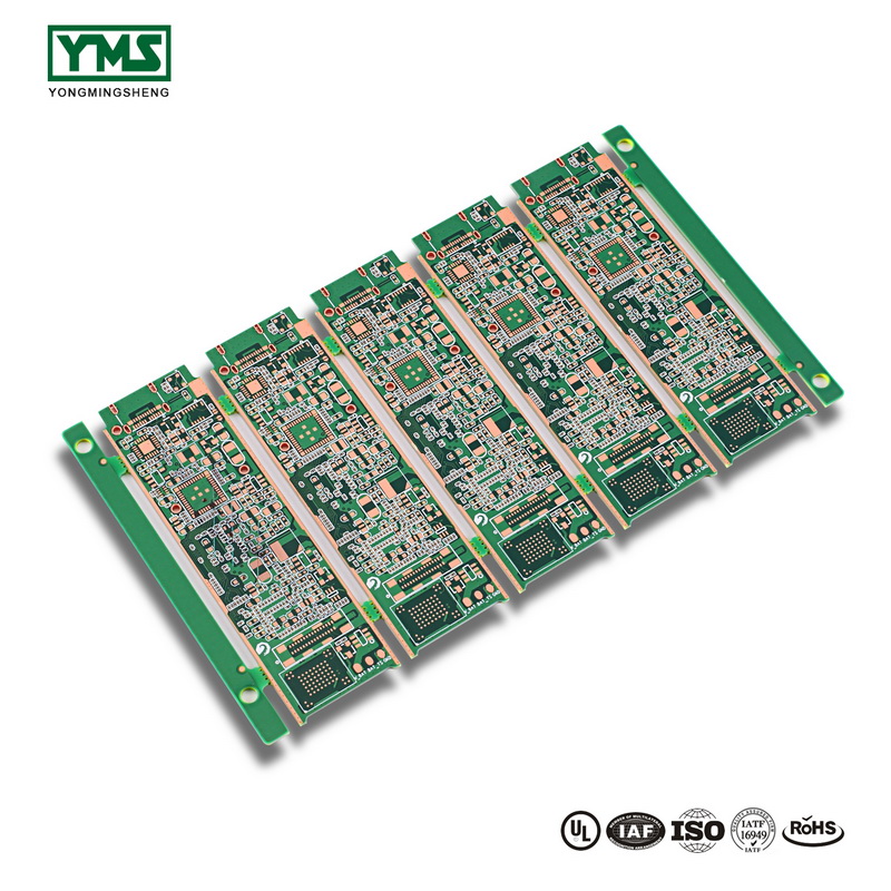
In the CAM production of all kinds of PCB, the personnel engaged in CAM production unanimously agree that the HDI mobile phone board is complicated in appearance and high in wiring density, which makes CAM production difficult and difficult to be completed quickly and accurately.
How to define SMD as the first difficulty in CAM production
In the process of PCB production, graphics transfer, etching and other factors will affect the final graphics, so we need to compensate the lines and SMD respectively according to the customer’s acceptance standards in CAM production. If we do not correctly define SMD, part of the finished product may be too small.
Customers often design 0.5mm CSP in HDI mobile phone board, and the size of the pad is 0.3mm, and some CSP pads have blind holes, and the pad corresponding to the blind hole is also 0.3mm, so that the CSP pad and the pad corresponding to the blind hole coincide or cross together.
In this case must be careful operation, beware of mistakes.(take genesis2000 as an example)
Specific production steps:
1. Close the drilling layer corresponding to blind hole and buried hole.
2. Define the SMD
3. Use FeaturesFilterpopup and Referenceselectionpopup functions to find the welding pad with include blind hole from the top layer and bottom layer, respectively, movetot layer and b layer.
4. Use ReferenceselecTIonpopup function on the t layer (the layer where the CSP pad is located) to select and delete the 0.3mm pad with blind hole phase Touch, and delete the 0.3mm pad in the CSP area of the top layer.According to the size, position and number of CSP pads designed by the customer, make a CSP by yourself and define it as SMD. Then copy the CSP pads to the TOP layer and add the pads corresponding to the blind holes in the TOP layer.B layer is made by similar method.
5. Find out other missing definitions or multiple definitions of SMD according to the network documents provided by the customer.
Compared with the conventional production method, the purpose is clear, the steps are few, this method can avoid misoperation, fast and accurate!
Removing the non-functional pad is also a special step in the HDI mobile phone board
Take the ordinary eight-layer HDI as an example, first remove the non-functional welding pad corresponding to the through-hole in the 2-7 layer, and then remove the non-functional welding pad corresponding to the 2-7 buried hole in the 3-6 layer.
The steps are as follows:
1. Use NFPRemovel function to remove the non-metallic holes of top and bottom layers corresponding to welding pads.
2. Close all drilling layers except the through hole and select NO from RemoveundrilLEDpads in NFPRemovel function to remove the 2– –7 layers of non-functional pads.
3. Close all drilling layers except layer 2– –7 buried holes. Select NO from NFPRemovel function for Removeundrilledpads to remove layer 3– –6 non-functional pads.
Using this method to remove non-functional welding pad, clear thinking, easy to understand, most suitable for the newly engaged in CAM production personnel.
About laser hole formation
HDI mobile plate of the blind hole is 0.1 mm or so commonly microporous, our company adopts CO2 laser, organic material can strongly absorb the infrared, through the thermal effect, the ablation into hole, but copper on infrared absorption is very small, and the melting point of copper is tall, CO2 laser can’t ablation copper foil, so use “conformalmask” process, with a copper etching liquid etched away laser drilling (CAM production exposed hole film).
At the same time to ensure that the outer layer (laser into the bottom of the hole) for copper, blind and buried hole spacing should be at least more than 4 mil, therefore, we must use the Analysis/FabricaTIon/Board – Drill – Checks find hole location does not meet the conditions.
Plug hole and resistance welding
In the laminating configuration of HDI, the secondary outer layer is generally made of RCC material with thin medium thickness and small amount of glue. According to the process experimental data, if the thickness of the finished plate is greater than 0.8mm, the metallized groove is greater than or equal to 0.8mmx2.0mm, and the metallized hole is greater than or equal to one of the three, two sets of plug hole files must be made.Namely divided into two plug hole, the inner layer with tree ester spade plug hole, the outer layer before welding resistance directly with welding ink plug hole.
In the process of resistance welding, there are often holes on SMD or next to SMD.The customer requires all the holes to be plugged, so when the welding resistance is exposed or half of the hole is exposed during the welding resistance exposure.
CAM staff must deal with this. In general, we first remove the hole. If the hole cannot be removed, follow the following steps:
1. Add a light transmission point 3MIL smaller than the single side of the finished hole on the cover hole position through the hole Covered.
2. Add a light transmission point of 3MIL larger than the single side of the finished hole in the welding resistance layer at the hole pass position of the window Touch.(in this case, the customer allows a little ink on the pad)
Appearance is made
HDI board is generally delivered as a jigsaw board with a complicated appearance. The customer attached a CAD drawing for the jigsaw board.If we use genesis2000 to draw according to the customer’s drawings, it is rather troublesome.
We can change the CAD file *.dwg to AutoCADR14/LT98/LT97DXF (*.dxf) and read *.dxf as normal genber file.While reading the shape, we can also read the size and position of the stamp hole, the positioning hole and the optical positioning point, which is fast and accurate.
Milling outline frame processing
When processing milling outline frame, in CAM production unless the customer requires exposure of copper, in order to prevent the plate edge over copper, according to the production specifications, the requirements to cut A little copper in the frame to the plate, so it is inevitable to appear as shown in figure 2 A!If the two ends of A do not belong to the same network, and the width of the copper sheet is less than 3mil (may not be able to do the figure), it will cause open circuit.
Such problems were not seen in the genesis2000 analysis, so an alternative approach was needed.We can make one more network comparison, and in the second comparison, cut the copper sheet near the border into the plate by 3mil more. If there is no open circuit in the comparison result, it indicates that both ends of A belong to the same network or the width is greater than 3mil (graphics can be made).If there is an opening, widen the copper sheet.