HDI PCB market supply and demand analysis and circuit advantages | YMSPCB
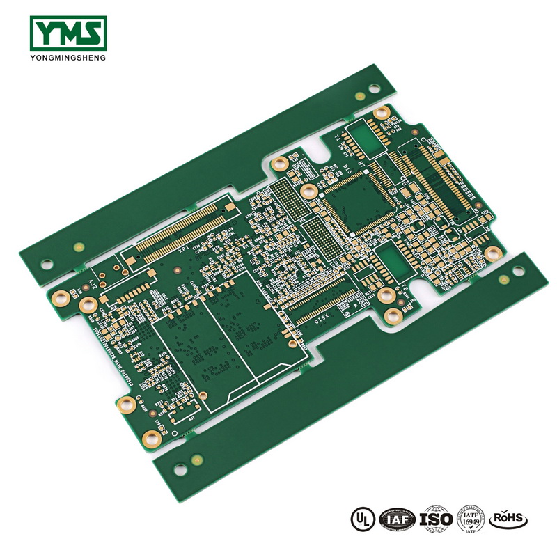
HDI (High Density Interconnector) printed circuit board (PCB) is a structural component composed of insulation and conductor wiring.Printed circuit boards are assembled with integrated circuits, transistors (transistors, diodes), passive components (resistors, capacitors, connectors, etc.) and various other electronic components when they are made into final products.By means of wire connection, electronic signal connection and function can be formed.A printed circuit board, therefore, is a platform for connecting components to form a base for connecting parts.
Printed circuit board is not a general end product, so the definition of the name is a little confused, for example: the PC used by the motherboard, called the motherboard but not directly called the circuit board, although there are circuit boards in the motherboard but not the same, so the industry evaluation of the two related but not the same.Another example: the news media call the integrated circuit board (IC board) because there are integrated circuit parts mounted on the circuit board, but it is not the same as the printed circuit board in essence.
Under the premise that electronic products tend to be multi-functional and complex, the contact distance of integrated circuit components shrinks accordingly, the speed of signal transmission is relatively increased, followed by the increase in the number of wiring, the length of interpoint distribution is locally shortened, which requires the application of high-density line configuration and micro-hole technology to achieve the goal.Wiring and bonding are basically difficult to achieve for single and double panels, so Circuit boards tend to be multilayered. Moreover, due to the continuous increase of signal lines, more power layers and connecting layers are necessary for design. All these make Multilayer Printed Circuit boards more common.
For the electrical requirements of high-speed signal, the circuit board must provide impedance control with alternating current characteristics, high frequency transmission capacity, reduce unnecessary radiation (EMI), etc.With Stripline, Microstrip structure, multilayer design became necessary.To reduce the quality of signal transmission, insulation materials with low dielectric coefficient and low attenuation rate will be adopted. In order to match the miniaturization and array of electronic components, the circuit board will constantly increase its density to meet the demand.The appearance of assembly methods of BGA (Ball Grid Array), CSP (Chip Scale Package), DCA (Direct Chip Attachment) and other group parts promotes the printed circuit board to the unprecedented high density state.
Any hole less than 150um in diameter is called Microvia in the industry. The circuit made by using the geometric structure technology of this microhole can improve the efficiency of assembly, space utilization and so on. At the same time, it is also necessary for the miniaturization of electronic products.
For such a structure of the circuit board products, the industry has a number of different names to call such a circuit board.For example, European and American companies used to call such products SBU (Sequence Build Up Process) because their programs were constructed in a sequential way.As for the Japanese companies, because the hole structure produced by such products is much smaller than the previous hole structure, the manufacturing technology of such products is called “Micro Via Process”.Some people call the traditional Multilayer Board MLB (Multilayer Board), so they call it BUM (Build Up Multilayer Board).
The IPC circuit board association of the United States in order to avoid confusion, and put forward this kind of product technology called HDI (High Density Intrerconnection) technology generic name, if translated directly into High Density interconnect technology.However, this does not reflect the characteristics of the circuit board, so most circuit board manufacturers refer to such products as HDI boards or the full Chinese name “high-density interconnection technology”.But because of the smoothness of the spoken word, some people call these products “high-density circuit boards” or HDI boards.
HDI PCB market supply and demand analysis
Demand for HDI boards has been driven by continued growth in mobile phone production
China plays an important role in the world mobile phone manufacturing industry.Since MOTOROLA introduced HDI boards in 2002, more than 90% of motherboards now use them.
A 2006 study by in-stat, a market research firm, predicted that global handset production would continue to grow at a rate of about 15 per cent over the next five years, with total global handset sales reaching 2bn by 2011.
China’s domestic HDI board capacity cannot meet the rapidly growing demand
In recent years, significant changes have taken place in the global production situation of HDI mobile phone board: except for famous mobile phone board manufacturers ASPOCOM and AT&S, most of the production capacity of HDI has been transferred from Europe to Asia.Asia, especially China, has become the world’s main supplier of HDI boards.
According to Prismark, China accounted for about 35 percent of global mobile phone production in 2006, and is expected to account for 50 percent of global mobile phone production by 2009, with HDI buying 12.5 billion yuan of mobile phone boards.In the case of the major players, China’s domestic players have less than 2% of global demand.Although some manufacturers have invested in production expansion, overall, China’s domestic HDI capacity growth still cannot meet the rapidly growing demand.
HDI circuit advantages
- Reduce PCB cost: when PCB density increases by more than eight layers, the cost of manufacturing with HDI will be lower than the traditional complex pressing process.
- Increased line density: interconnection of conventional circuit boards and components
- It is beneficial to the use of advanced construction technology
- Better electrical performance and signal accuracy
- Better reliability
- The thermal properties can be improved
- Improve rf interference/electromagnetic interference/electrostatic release (RFI/EMI/ESD)
- Increase design efficiency
