What are the advantages of HDI in PCB| YMS
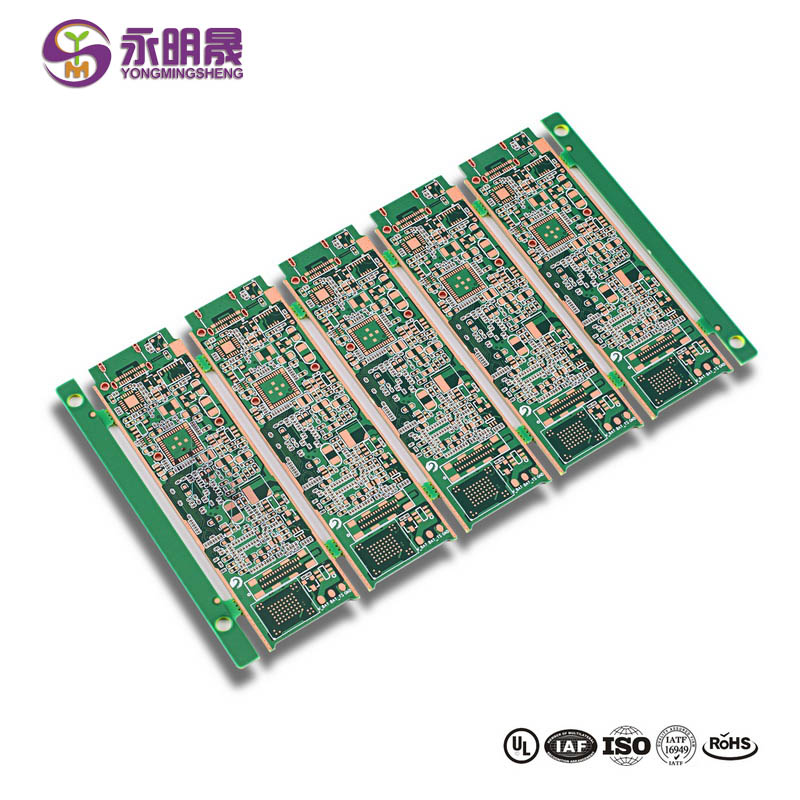
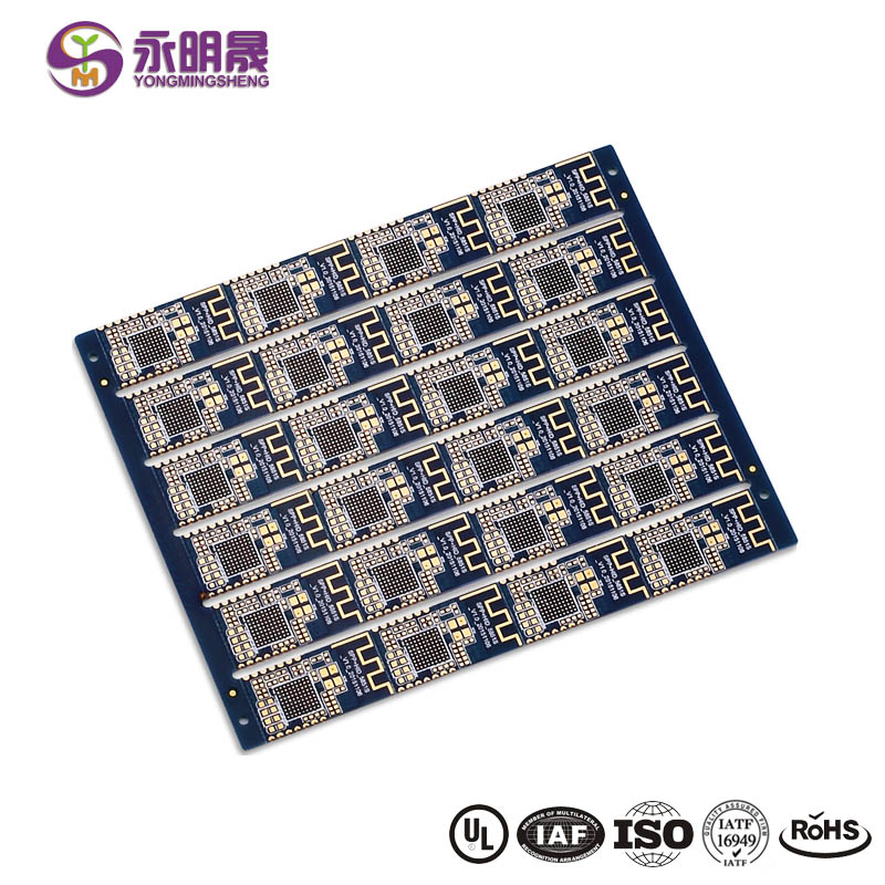
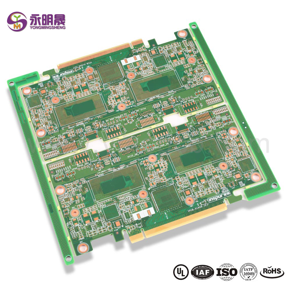
HDI stands for high Density interconnect and is a form of printed circuit board (PCB) that uses microblind buried hole technology to produce a high density circuit board.
Electronic design is constantly improving the performance of the whole machine, but also trying to reduce its size. From cell phones to smart weapons, “small” is a constant pursuit. High density integration (HDI) technology enables end product designs to be miniaturized while meeting higher standards of electronic performance and efficiency. HDI is widely used in mobile phones, digital cameras, MP4, notebook computers, automotive electronics and other digital products, among which mobile phones are the most widely used. HDI board is generally manufactured by build-up method. The more times of stacking, the higher the technical level of the board. Ordinary HDI board is basically one layer, high order HDI uses two or more layers of technology, at the same time the use of stacking holes, electroplating hole filling, laser direct drilling and other advanced PCB technology. Advanced HDI boards are mainly used in 5G mobile phones, advanced digital cameras, IC boards, etc.The advantages and applications of HDI PCBs.
· Compact design
The combination of micro vias, blind vias, and buried vias reduces the board space greatly. With the support of HDI technologies, a standard 8-layers through-hole PCB can be simplified to a 4-layer HDI PCB with the same functions.
· Excellent signal integrity
With small vias, all stray capacitance and inductance will get reduced. And the technology of incorporating bind vias and via-in-pad helps to shorten the length of the signal path. These will lead to faster signal transmission and better signal quality.
· High reliability
HDI technology makes route and connect easier, and offers PCBs better durability and reliability in hazardous conditions and extreme environment.
· Cost-effective
There needs much more manufacturing cost when the boards are beyond 8-layer if using traditional pressing processes. But HDI technology can reduce the cost and keep the function purpose.
HDI PCBs have been used widely to reduce the entire size and weight of final products while enhancing the electrical performance. For these medical devices like pacemakers, miniaturized cameras, and implants, only HDI techniques are capable of supplying small packages with fast transmission rates.
You May Like
HDI PCB 12 Layer
HDI pcb 3+N+3 Laser
HDI pcb any layer
People also ask
1. What are the advantages and disadvantages of flexible circuit board


