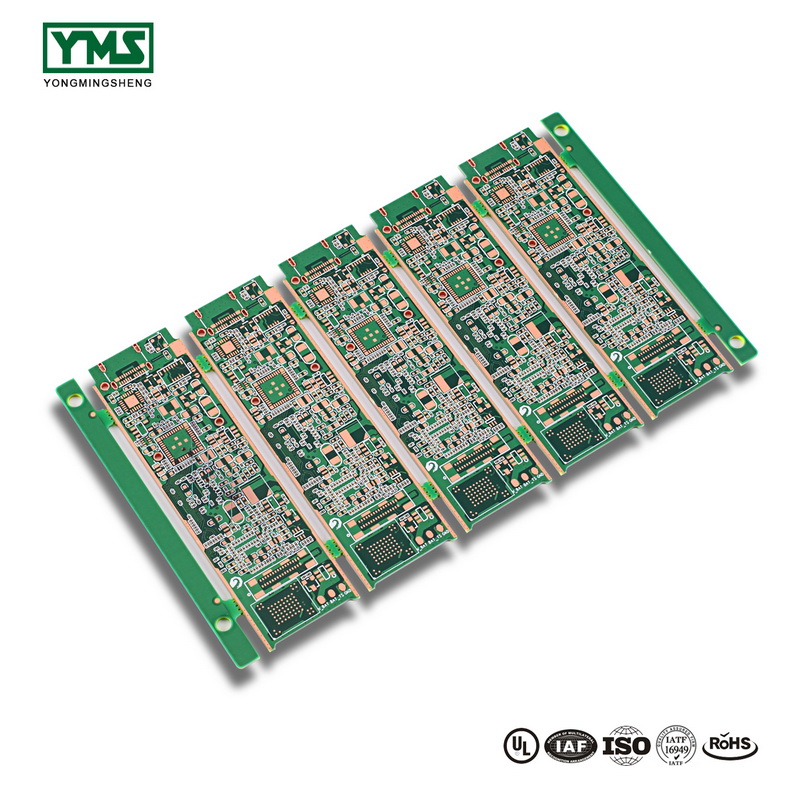
What are the copper cladding skills of PCB?
Chinese PCB manufacturer tells you
The main function of PCBS is “backflow and shielding”.PCB copper cladding is mainly carried out by means of grid.
Double-sided PCB with copper cover thickness of about 35um (1.4mil);50um is uncommon;
The surface layer of PCBS is 35um (1.4mil) and the inner layer is 17.5um (0.7mil).
PCB copper thickness is also indicated in OZ (OZ).The advantages of PCB copper coating are “improving power efficiency, reducing high-frequency interference and improving aesthetics”.
Told so much knowledge of PCB copper cladding, then PCB copper cladding skills and Settings?Yongmingsheng PCB factory is now going to introduce the technique and setting of PCB copper coating..
PCB copper covering technique:
1, if the PCB is more, have SGND, AGND, GND, etc., will be depending on the position of PCB board face, respectively to the main “to” independent copper clad as reference point, to digital and analog to separate apply copper from a few words, at the same time before the copper clad, first of all, bold corresponding power cords: 5.0 V, 3.3 V, etc., as a result, a number of different shapes are formed more deformation structure.
2. For single point connection at different locations, the method is to connect through 0 ohm resistance or magnetic bead or inductance;
3. If the crystal oscillator is covered with copper near the crystal oscillator, the crystal oscillator in the circuit is a high-frequency transmitting source. The method is to lay copper around the crystal oscillator, and then ground the shell of the crystal oscillator separately.
4, island (dead zone) problem, if you feel very big, then define a hole to add in the cost of not much.
5, in the beginning of wiring, should be treated as the same ground wire, wire should be good, can not rely on copper after adding holes to eliminate as a connection pin, this effect is very bad.
6. It is best not to have a sharp Angle on the board (=180 degrees), because from the point of view of electromagnetism, this constitutes a transmitting antenna! For others, there will always be an impact is just big or small, I suggest using the edge of the arc along the edge.
7, multi-layer board middle layer wiring empty area, do not apply copper.Because it’s hard for you to make this copper “well grounded.”
8. The metal inside the equipment, such as metal radiator and metal reinforcement strip, must be “well grounded”.
9. The cooling metal block of the three-terminal regulator must be well grounded.The ground isolation belt near the crystal vibration must be well grounded.In a word, if the grounding problem is properly handled, the copper coating on the PCB will definitely bring more advantages than disadvantages. It can reduce the backflow area of the signal line and reduce the external electromagnetic interference of the signal.


