Which kind of PCB board needs gold and goldfinger | YMSPCB
First of all, what is sinker gold?
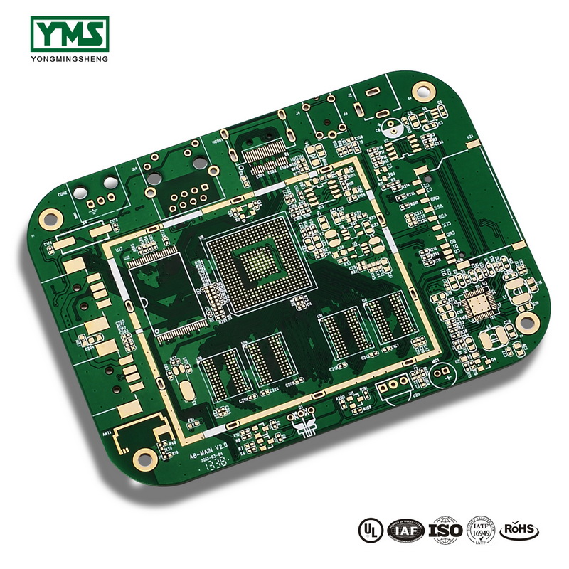
The copper on the Printed circuit board is mainly red copper, copper welding spot in the air is easy to be oxidized, which will cause the conductivity is eating tin bad or bad contact, reduce the performance of the printed circuit board, so it is necessary to copper solder surface treatment;
Sink gold is above gold-plated, gold can effectively block copper metal and air prevent oxidation off, so sink gold is a kind of surface oxidation treatment, is through chemical reaction on the surface of copper covered with a layer of gold, also known as gold.
So what is a goldfinger?
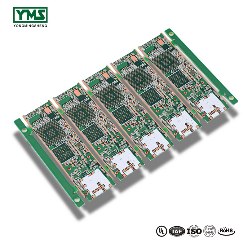
Gold fingers pcb: Let’s put it more bluntly, a brass contact, or a conductor. Specifically, the parts of the memory stick connected to the memory slot, all the signals are sent by the golden finger, which is composed of numerous yellow conductive contacts, whose surface is gold-plated and arranged like fingers, hence the name.
The advantage of gold sinking process is that the printed line surface deposition color is very stable, good brightness, coating is very smooth, very good weldability.
Generally, the thickness of gold deposit is 1-3 Uinch, which can be basically divided into four stages: pretreatment (oil removal, micro-corrosion, activation and later immersion), nickel deposit, gold deposit, and post-treatment (waste gold water washing, DI washing and drying).
However, the cost of gold sinking process is higher than that of other tin spraying processes. If the thickness of the gold exceeds the standard process of the plate making factory, the cost is even more expensive. Of course, if you have higher requirements on the weldability and electrical properties of the board, that is another matter.
Such as: your printed circuit board with the fingers need to sink gold, or the line width of the board/pad spacing is not enough, so it is best to do heavy + gold plating process for the finger, this printed circuit board welding is very good, circuit performance is also stable, bonding pad will not fall off, not bad contact, there will be no short circuit etc. Phenomenon, at the same time also is very shock drop, of course, we won’t fall off the board.
There is a kind of situation is the printed circuit board has golden finger, but the board outside the golden finger can choose according to the situation spray tin process, that is, spray tin + gold-plated finger process, in the printed circuit board wire width and solder pad spacing is sufficient, welding requirements are not high, can effectively reduce the production cost, and does not affect the use of the board.
But if the wire width of the board and the gap between the welding pad is insufficient, then this situation using spray tin process will increase the production difficulty, will appear tin bridge and other short circuit situation will be more, will also give cash finger often insert peel, resulting in poor contact.
So we can according to the actual situation of their printed circuit boards, to choose their own baord manufacturing process, that is, control the cost and can not affect the use of the board.
Yongmingsheng technology co., LTD. is a high-tech company integrating printed circuit board development, design, proofing, production (processing), testing, production and sales.
The main products are: hard gold PCB, metal core PCB, Flex-Rigid,reasonable price.
Since the establishment of the company, from the original professional circuit board processing, to expand the production of flexible circuit board, rigid circuit board, etc. We have been making progress, we have been committed to become a high quality PCB manufacturer and service provider.

