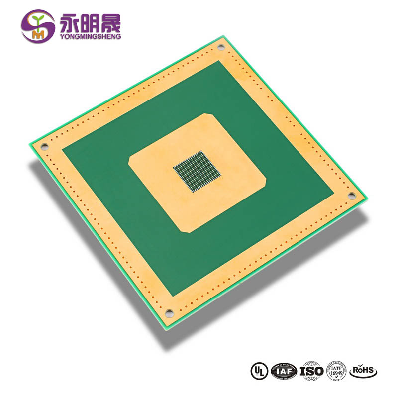
RF&Microwave PCB manufacturing microwave high frequency | YMSPCB
What is RF & Microwave PCB and Microwave PCB Different from Ordinary PCB
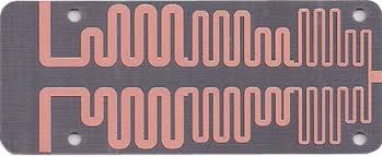
Radio frequency (RF) and microwave PCB’s are a type of PCB designed to operate on signals in the medium frequency to extremely high frequency ranges (megahertz to gigahertz). These ranges are used for communication signals in everything from mobile phones to military radars.
The materials used are advanced composites with very specific characteristics for dielectric constant (Er), loss tangent, and CTE (co-efficient of thermal expansion). These materials can be mixed in the same Stack-Up for optimal performance and economics.
RF PCB standard:
- Low power RF PCBmainly uses standard FR4 material (good insulation properties, uniform material, dielectric constant ε=4, 10%).
- In the RF PCB design, each component should be closely arranged to ensure the shortest connection.
- For a mixed-signal PCB, the RF and analog partsshould be far away from the digital part (the distance is usually more than 2cm, at least 1cm), and the ground of the digital part should be separated from the RF part.
- When selecting components to work in a high-frequency environment, use SMD(Surface Mounted Devices) as much as possible. SMD are small in size, and the component pins are generally very short.
This article provides guidelines and suggestions for radio frequency (RF) printed circuit board (PCB) design and layout, including some discussion of mixed-signal applications, such as digital, analog, and RF components on the same PCB. The content is organized by topic areas and provides “best practice” guidelines, which should be applied in conjunction with all other design and manufacturing guidelines. These guidelines may also apply to specific components, PCB manufacturers, and materials.
RF Transmission Lines
Many of Maxim’s RF components require a transmission line with controlled impedance to transmit RF power to IC pins on the PCB. These transmission lines can be implemented on the outer layer (top or bottom layer) or buried in an inner layer. Guidelines for these transmission lines include discussions of microstrip lines, strip lines, coplanar waveguides (grounded), and characteristic impedance. It also introduces transmission line bending angle compensation and the layer change of the transmission line.
The Microstrip
This transmission line includes a fixed-width metal trace (conductor) and a ground area located directly underneath (on the adjacent layer). For example, a microstrip on layer 1 (top metal) requires a solid ground area on layer 2 (Figure 1). The width of the trace, the thickness of the dielectric layer, and the dielectric determine the characteristic impedance (usually 50Ω or 75Ω)

Figure 1. Microstrip line (3D view)
The Stripline
This line includes a fixed-width trace on the inner layer and solid ground areas above and below.
The conductor can be located in the middle of the ground area (Figure 2) or have a certain offset (Figure 3). This method is suitable for the inner radiofrequency routing.

Figure 2. Stripline (end view)

Figure 3. Offset stripline. A variant of stripline for PCBs with different layer thicknesses (end view)
Coplanar Waveguide (Grounded)
A coplanar waveguide provides better isolation between adjacent RF lines and other signal lines (end view). This medium includes an intermediate conductor and grounding areas on both sides and below (Figure 4).

Figure 4. Coplanar waveguide provides better isolation between adjacent RF lines and other signal lines
Via “fences” are recommended on both sides of the coplanar waveguide, as shown in Figure 5. This top view provides an example of installing a row of ground vias in the top metal ground area on each side of the intermediate conductor. The loop currents induced on the top layer are shorted to the underlying ground plane.

Figure 5. Via fences on both sides of the coplanar waveguide
Request Multilayer PCB Quote
Contact Us
Characteristic Impedance
Several calculation tools can properly set the signal conductor line width to achieve the target impedance. However, we should be careful when entering the dielectric constant of the circuit board layers.
The outer layer of typical PCBs contain less glass fiber than the inner layer, so the dielectric constant is lower. For example, the dielectric constant of FR4 material is generally εR = 4.2, while the outer substrate (prepreg) layer is generally εR = 3.8. The example below is for reference only. The metal thickness is 1oz copper (1.4 mils, 0.036mm).
Table 1. Example of characteristic impedance:

When the transmission lines are required to be bent (change direction) due to wiring constraints, the bending radius used should be at least three times the width of the intermediate conductor. In other words:
Bending radius ≥ 3 × (line width).
This will minimize the characteristic impedance change of the corner.
If it is impossible to achieve gradual bending, the transmission line can be bent at right angles (non-curved), as shown in Figure 6. However, this must be compensated to reduce the sudden change in impedance caused by the increase in the local effective line width when passing through the bending point. The standard compensation method is the miter angle , as shown in the figure below. The formula of Douville and James gives the best microstrip right-angle miter:
![]()
In the formula, M is the ratio(%) of mitered and non-mitered corners. The formula is independent of the dielectric constant, and the constraint condition is w/h ≥ 0.25.
Similar methods can be used for other transmission lines. If there is any uncertainty about the correct compensation method, and the design requires a high-performance transmission line, we should use an electromagnetic simulator to model the bend.

Figure 6. If gradual bending is not possible, the transmission line can be bent at a right angle.
The Layer changes of transmission lines
Suppose the layout constraints require changing the transmission line to a different circuit board layer. In that case, it is recommended to use at least two vias for each transmission line to minimize the inductive loading. A pair of vias will effectively reduce the transmission inductance by 50%, and we should use the largest diameter via with the same width as the transmission line. For example, for a 15-mil microstrip line, the via diameter (finished plating diameter) should be 15 mil to 18 mil. If the space does not allow the use of large vias, we should use three transition vias with smaller diameters.
Request RF PCB Quote
Contact Us
Signal Line Isolation
We must be careful to prevent accidental coupling between signal lines. The following are examples of potential coupling and preventive measures:
- RF transmission lines:The distance between the transmission lines should be as large as possible and should not be close to each other over a long distance. The smaller the distance between each other and the longer the distance between parallel traces, the greater the coupling between parallel microstrip lines. The traces on different layers should have ground areas to keep them separate. Transmission lines carrying high power should be as far away from other transmission lines as possible. Grounded coplanar waveguides provide excellent line-to-line isolation. It is unrealistic for the isolation better than -45dB between RF lines on a small PCB.
- High-speed digital signal lines:These signal lines should be arranged independently on a different circuit board layer from the RF signal lines to prevent coupling. Digital noise (from clocks, PLLs, etc.) will be coupled to the RF signal line and then modulated to the radio frequency carrier. In some cases, digital noise will be upconverted or
- VCC/power lines:These lines should be arranged on a dedicated layer. Appropriate decoupling or bypass capacitors should be installed at the main VCC distribution node and VCC branch. The bypass capacitor must be selected based on the overall frequency response of the RF IC and the expected frequency distribution of digital noise caused by the clock and PLL. These traces should also be kept isolated from the RF lines. Otherwise, they will emit larger RF power.
Ground Area
If layer 1 is used for radio frequency components and transmission lines, it is recommended to use a solid (continuous) ground area on layer 2. For strip lines and offset strip lines, the upper and lower intermediate conductors require grounding areas. These areas must not be shared or allocated to signal or power networks but must be allocated to the ground. Sometimes limited by design conditions, a local ground area on a specific layer must be located under all radio frequency components and transmission lines. The ground area must not be disconnected under the transmission line.
A large number of ground vias should be placed between different layers of the RF part of the PCB. This helps prevent ground current loops from increasing parasitic ground inductance. Vias also help prevent cross-coupling of RF signal lines and other signal lines on the PCB.
Special Considerations for power and ground layers
For the circuit board layers allocated to the system power (DC power) and ground, the loop current of the components must be considered. The general principle is to avoid placing signal lines on the circuit board layer between the power and ground layers.

Figure 7. Incorrect circuit board layer assignment: There are signal layers between the power layer and the ground current loop on the ground layer. Bias line noise can couple to the signal layers.

Figure 8. Better layer assignment: There is no signal layer between the power layer and the ground layer.
Power (Bias) Traces and Power Decoupling
If the component has multiple power connections, a common practice is to use power wiring in a “star” configuration (Figure 9). Install larger decoupling capacitors (tens of µF) at the “root” node of the star configuration, and install smaller capacitors on each branch. The value of these small capacitors depends on the operating frequency of the RF IC and its specific functions (i.e., decoupling between stages and the main power supply). An example is shown below:

Figure 9. If a component has multiple power connections, the power wiring can be in a star configuration.
Compared with the configuration in which all pins are connected to the same power network in series, the “star” configuration avoids long ground loops. Long ground loops will cause parasitic inductance, which can cause unexpected feedback loops. The key consideration for power supply decoupling is that the DC power supply must be electrically connected to an AC ground.
Selection of Decoupling and Bypass Capacitors
Due to the existence of self-resonant frequency (SRF), the capacitor’s effective frequency range, in reality, is limited. SRF can be obtained from the manufacturer, but sometimes must be characterized by direct measurement. Above SRF, the capacitor is inductive, so it has no decoupling or bypassing function. If broadband decoupling is required, the standard approach uses multiple (capacitance values) of increased capacitors, all in parallel. The SRF of a small capacitor is generally larger (for example, the SRF of a 0.2pF, 0402 SMT package capacitor = 14GHz). The SRF of a large capacitor is generally smaller (for example, the SRF of a 2pF capacitor in the same package = 4GHz). Table 2 lists typical configurations.

Table 2. Effective frequency range of capacitors
Bypass capacitor layout considerations
Since the power lines must be AC ground, it is essential to minimize the parasitic inductance of the AC ground loop. The component layout or placement direction may cause parasitic inductance, such as the ground direction of decoupling capacitors. There are two ways to place the bypass capacitor, as shown in Figure 10 and Figure 11:

Figure 10. The total area of the bypass capacitor and related vias is the smallest.

Figure 11. This configuration requires a larger PCB area.
In this configuration, connecting the VCC pad on the top layer to the via hole of the inner power supply region (layer) may hinder the AC ground current loop, forcing a longer loop, resulting in higher parasitic inductance. Any AC flowing into the VCC pin passes through the bypass capacitor, reaches its ground side, and then returns to the inner ground plane. In this configuration, the total footprint of the bypass capacitor and related vias is the smallest. In another configuration, the AC ground loop is not restricted by the vias in the power supply area. Generally speaking, this configuration requires a slightly larger PCB area.
Grounding of crowbar-connected components: For crowbar-connected (grounded) components such as power supply decoupling capacitors, it is recommended to use at least two ground vias for each component (Figure 12), reducing the influence of via parasitic inductance. The short-circuit connection component group can use via grounding “island.”

Figure 12. Using at least two ground vias per component can reduce the effect of via parasitic inductance.
IC Ground Area (“pad”)
Most ICs require a solid ground area on the component layer (the top or bottom layer of the PCB) directly below the component. This ground area will carry DC and RF return flow through the PCB to the distributed ground area. The second function of the component “ground pad” is to provide a heat sink, so the pad should include the maximum number of vias as permitted by the PCB design rules.
In the example shown in the figure below, a 5 × 5 via array is installed in the middle ground area (on the component layer) directly below the RF IC (Figure 13). Where other layout considerations allow, the maximum number of vias should be used. These vias are ideal vias (through the entire PCB). These vias must be plated. If possible, use the thermal paste to fill the vias to improve heat dissipation (fill the thermal paste after plating the vias before finally plating the circuit board).

Figure 13. A 5 × 5 via array on the middle ground area directly below the RF IC
All high-frequency PCB operating beyond 100 MHz are termed as RF PCBs whereas a Microwave RF PCB operates above 2GHz. The development procedures involved in RF PCBs are different as compared to conventional PCBs. RF Microwave PCBs are much more sensitive towards various parameters which have no effects over ordinary PCBs. So, the development has too carried out in a controlled environment with the required expertise.
RF Microwave PCB applications
RF Microwaves PCBs are used in various wireless technology based products. If you are working on robotics, smartphones, security applications or sensors, you need to select a perfect RF Microwave PCB for your product.
With the advancement of technology, every day new designs and products are entering the market. These advancements have brought about a significant revolution in electronics. For a product developer, it is of great interest to find a suitable PCB for his product which ensures a smooth working and long life.
Finding perfect RF Microwave PCB for your project can be stressful especially when it comes to choosing suitable PCB material. For a project developer, it is of great interest that his PCB may be of high-grade material with proper functioning and it should be delivered in time.
The parameters such as RF Microwave energy levels, Operating frequency, operating temperature range, Current and Voltage requirements are of great importance when choosing perfect material for PCB material.
When getting started with your PCB manufacturing, make sure you have chosen the right specifications for your PCB. Classical High-frequency RF Microwave frequencies were single layer PCB constructed on the dielectric. However, with the evolution in RF Microwave PCB designs, many technologies have emerged during the past few decades.
Why do you need to focus on choosing the right manufacturer?
Ordering PCB manufacturing from a high tech equipped facility can be more beneficial than getting it manufactured in a low-cost manufacturing facility with low-grade material used.
RF PCBs are highly sensitive towards factors such as noise, impedance, electromagnetism, and ESds. High-quality PCB manufacturers focus on eliminating any affecting factors during manufacturing. A poor quality RF Microwave PCB is not expected to sustain for long, and that’s why choosing a perfect RF PCB manufacturer can alter your product experience.
Today, most of the modern RF PCB manufacturing facilities use Computer Aided Engineering software simulation programs for PCB manufacturing. The best advantage of CAD-based RF Microwave PCB manufacturing is that it has simulation models of various brands and PCB models with proper product specifications.
These parameters are essential in the production of a standardized RF Microwave PCB and ensure reliability. Furthermore, the machines also support manual functioning, allowing the operator to perform manual operations.
So, it is evident that RF Microwave PCB manufacturing is not as simple as it seems.
Benefits of getting your RF PCB manufactured by YMS
RF Microwave PCBs are not easy to manufacture unlike regular PCBs and requires detailed monitoring of various factors, being an experienced RF Microwave PCB manufacturer, YMS has developed the experience of handling RF projects and knows precisely how to incorporate these factors. The quality products and satisfactory experience of our clients uplift our image.
Trusting a PCB manufacturer with your sensitive product can be difficult, and we truly understand that. YMS not only assists its clients during the manufacturing process but offers detailed technical support even after the manufacturing of PCB.
We ensure that your PCB manufacturing is not just developed but the product functions exactly as required and before manufacturing, the technical experts at YMS analyze the complete design for any possible flaws or cushion for improvements. Accordingly, customer concerns are considered, and a reliable product is developed.
If, a design lacks over any specifications or required featuring, our team is liable to discuss with the customer and offer alternatives. Furthermore, the client is saved from the hustle of testing as our testing team performs various tests at your custom RF Microwave PCB and makes sure that it serves the purpose.
YMS Microwave & RF PCB manufacturing capabilities:
| YMS Microwave/RF PCB manufacturing capabilities overview | ||
| Feature | capabilities | |
| Layer Count | 2-14L | |
| Available Microwave/RF PCB Technology | Through hole with Aspect Ratio 16:1 | |
| buried and blind via | ||
| Mixed Dielectric Boards (PTFE+FR-4 combinations ) | ||
| Suitable Microwave/RF Materials available : PTFE, FR4, Polymide, Polyester, Ceramic | ||
| Tight Etch Tolerances on Critical RF Features:+/- .0005″ standard tolerance for unplated 0.5oz copper | ||
| Multilevel cavity constructions, Copper coins and slugs, Metal Core & Metal Back, Thermally conductive laminates,Edge Plating, etc. | ||
| Thickness | 0.3mm-8mm | |
| Minimum line Width and Space | 0.075mm/0.075mm(3mil/3mil) | |
| BGA PITCH | 0.35mm | |
| Min laser Drilled Size | 0.075mm(3nil) | |
| Min mechanical Drilled Size | 0.15mm(6mil) | |
| Aspect Ratio for laser hole | 0.9:1 | |
| Aspect Ratio for through hole | 16:1 | |
| Surface Finish | Suitable Microwave/RF PCB urface finishes: Electroless Nickel, Immersion Gold, ENEPIG, Lead free HASL,Immersion Silver | |
| Via Fill Option | The via is plated and filled with either conductive or non-conductive epoxy then capped and plated over(VIPPO) | |
| Copper filled, silver filled | ||
| Laser via copper plated shut | ||
| Registration | ±4mil | |
| Solder Mask | Green, Red, Yellow, Blue, White, Black, Purple, Matte Black, Matte green.etc. | |
Learn more about YMS products
Bendable PCB 1Layer
Metal clad pcb
Aluminum pcbs
Thick Copper PCB 10 Layer
RF&Microwave PCB manufacturing microwave high frequency | YMSPCB Related Video:
