Rigid flex pcb single sided fpc blind via core+core stackup| YMSPCB
Different Design Rules Apply to Rigid-Flex PCB Design
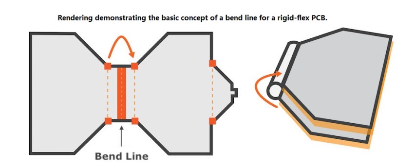
Flexible circuits always have bend lines that affect routing. Because of the potential for material stress, you cannot place components or vias close to the bend line.
And even when components are properly located, bending flex circuits places repeated mechanical stresses on surface-mount pads and through holes. Your team can reduce those stresses by using through-hole plating and by bolstering pad support with additional coverlay to anchor the pads.
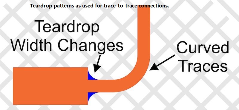
As you design your trace routing, follow practices that reduce stress on your circuits. Use hatched polygons to maintain flexibility when carrying a power or ground plane on your flex circuit. You should use curved traces rather than 90° or 45° angles and use teardrop patterns to change trace widths.
YMS Rigid Flex PCB manufacturing capabilities:
| YMS Rigid Flex PCB manufacturing capabilities overview | ||
| Feature | capabilities | |
| Layer Count | 2-20L | |
| Rigid-Flex Thickness | 0.3mm-5.0mm | |
| PCB thickness in flex section | 0.08-0.8mm | |
| copper Thickness | 1/4OZ-10OZ | |
| Minimum line Width and Space | 0.05mm/0.05mm(2mil/2mil) | |
| Stiffeners | Stainless steel,PI, FR4 ,Aluminum etc. | |
| Material | Polyimide Flex+FR4,RA copper, HTE copper, polyimide, adhesive,Bondply | |
| Min mechanical Drilled Size | 0.15mm(6mil) | |
| Min laser Holes Size: | 0.075mm(3mil) | |
| Surface Finish | Suitable Microwave/RF PCB urface finishes: Electroless Nickel, Immersion Gold, ENEPIG, Lead free HASL,Immersion Silver.etc. | |
| Solder Mask | Green, Red, Yellow, Blue, White, Black, Purple, Matte Black, Matte green.etc. | |
| Covrelay (Flex Part) | Yellow Coverlay, WhiteCoverlay,Black Coverlay | |
Learn more about YMS products
PCB bare board
Multilayer PCB buried and blind
Flexible Circuit Board 2layer
High Tg material PCB 6 Layer
Flexible Printed Circuit Board
Read more news
Rigid flex pcb single sided fpc blind via core+core stackup| YMSPCB Related Video:


