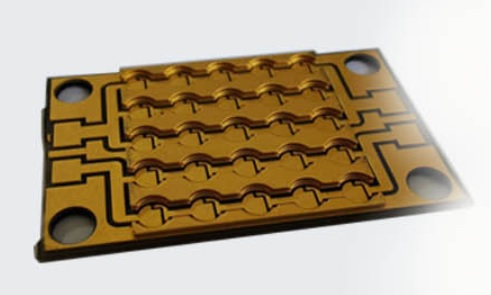
Extreme Copper PCB 2 Layer 10 0z Heavy Copper Board| YMS PCB
Product Detail
The construction of a heavy copper circuit endows a board with benefits such as:
- Increased endurance to thermal strains.
- Increased current carrying capacity.
- Increased mechanical strength at connector sites and in PTH holes.
- Use of exotic materials to their full potential without circuit failure.
- Reduced product size by incorporating multiple copper weights on the same layer of circuitry .
- Heavy copper plated vias carry higher current through the board and help to transfer heat to an external heatsink.
YMS Heavy copper PCB manufacturing capabilities:
| YMS Heavy copper PCB manufacturing capabilities overview | ||
| Feature | capabilities | |
| Layer Count | 1-30L | |
| Base Material | FR-4 Standard Tg, FR4-mid Tg,FR4-High Tg | |
| Thickness | 0.6 mm – 8.0mm | |
| Maximum Outer Layer Copper Weight (Finished) | 15OZ | |
| Maximum Inner Layer Copper Weight (Finished) | 30OZ | |
| Minimum line Width and Space | 4oz Cu 8mil/8mil; 5oz Cu 10mil/10mil; 6oz Cu 12mil/12mil; 12oz Cu 18mil/28mil; 15oz Cu 30mil/38mil .etc. | |
| BGA PITCH | 0.8mm(32mil) | |
| Min mechanical Drilled Size | 0.25mm(10mil) | |
| Aspect Ratio for through hole | 16:1 | |
| Surface Finish | HASL, Lead free HASL,ENIG,Immersion Tin, OSP, Immersion Silver, Gold Finger, Electroplating Hard Gold, Selective OSP,ENEPIG.etc. | |
| Via Fill Option | The via is plated and filled with either conductive or non-conductive epoxy then capped and plated over(VIPPO) | |
| Copper filled, silver filled | ||
| Registration | ±4mil | |
| Solder Mask | Green, Red, Yellow, Blue, White, Black, Purple, Matte Black, Matte green.etc. | |
You May Like:
1、What are the precautions for heavy copper PCB wiring
2、What are the specifications of heavy copper PCB
3、What are the heavy copper PCB materials
Learn more about YMS products

Flex Printed Circuit 2Layer

Hard Gold (BGA) Board

High speed PCB
Product Tags
Extreme Copper PCB 2 Layer 10 0z Heavy Copper Board| YMS PCB Related Video: