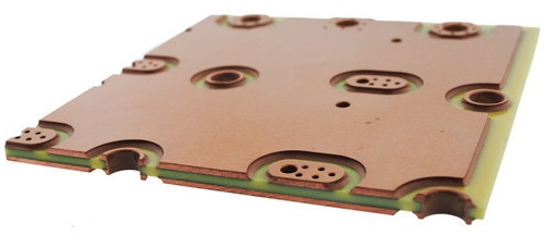
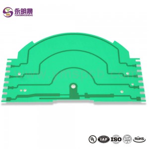
heavy copper pcb 4 Layer (4/4/4/4OZ) Black Soldermask Board| YMS PCB
What is heavy copper PCB?
This PCB classic is the first choice when high currents are unavoidable: the thick copper PCB, manufactured in genuine etching technology. Thick copper PCBs are characterised by structures with copper thicknesses from 105 to 400 µm. These PCBs are used for large (high) current outputs and for optimisation of the thermal management. The thick copper allows large PCB-cross-sections for high current loads and encourages heat dissipation. The most common designs are multilayer or double-sided.
While there is no standard definition of Heavy Copper, it is generally accepted that if 3 ounces (oz) of copper or more is used on the internal and external layers of a printed circuit board, it is called a heavy copper PCB. Any circuit with a copper thickness of more than 4 oz per square foot (ft2) is also categorized as a heavy copper PCB. Extreme copper means 20 oz per ft2 to 200 oz per ft2.
A heavy copper PCB is identified as a PCB with a copper thickness 3 oz per ft2 to 10 oz per ft2 in the outer and inner layers. A heavy copper PCB is produced with copper weights ranging from 4 oz per ft2 to 20 oz per ft2. The improved copper weight, along with a thicker plating and appropriate substrate in the through-holes can change a weak board into a long-lasting and dependable wiring platform. Heavy copper conductors can increase the entire PCB thickness considerably. The copper thickness should always be considered during the circuit design stage. The current-carrying capacity is determined from the width and thickness of heavy copper.
The primary benefit of heavy copper circuit boards is their capability to survive frequent exposure to excessive current, elevated temperatures and recurring thermal cycling, which can destroy a regular circuit board in seconds. The heavy copper board has a high tolerance capacity, which makes it compatible with applications in rough situations such as, defense and aerospace industry products.
Some of the added advantages of heavy copper circuit boards are:
Compact product size due to several copper weights on the same layer of circuitry
Heavy copper-plated vias pass the elevated current through the PCB and assist in transferring the heat to an outer heat sink
Difference between a Standard PCB and Thick Copper PCB
Standard PCBs can be produced with copper etching and plating processes. These PCBs are plated to add copper thickness to planes, traces, PTHs, and pads. The amount of copper used in the production of standard PCBs is 1oz. In the production of heavy copper PCB, the amount of copper used is greater than 3oz.
For standard circuit boards, copper etching and plating techniques are utilized. However, heavy copper PCBs are produced via differential etching and step platting. Standard PCBs perform lighter activities while heavy copper boards perform heavy duties.
Standard PCBs conduct lower current while heavy copper PCBs conduct higher current. Thick copper PCBs are ideal for high-end applications due to their efficient thermal distribution. Heavy copper PCBs have better mechanical strength than standard PCBs. Heavy copper circuit boards enhance the capability of the board in which they are utilized.
Other features that make thick copper PCBs different from other PCBs
Copper weight: This is the main distinguishing feature of heavy copper PCBs. Copper weight refers to the weight of the copper used in a square foot area. This weight is usually measured in ounces. It indicates the copper’s thickness on the layer.
Outer layers: These refer to the external copper layers of the board. Electronic components are usually bonded to the external layers. The external layers begin with copper foil which is coated with copper. This helps to increase the thickness. The copper weight of the external layers is preset for standard designs. Heavy copper PCB manufacturer can alter the weight and thickness of the copper to suit your requirement.
Inner layers: The dielectric thickness, as well as the copper mass of the internal layers, is predefined for the standard projects. However, the copper weight and thickness in these layers can be adjusted based on your needs.
Heavy copper PCBs are used for multiple purposes such as in planar transformers, heat dissipation, high power distribution, power converters, etc. There is an increased demand for heavy copper-clad boards in computer, automotive, military, and industrial controls.
Heavy copper printed circuit boards are also used in:
Power supplies, power converters
Power distribution
YMS Heavy copper PCB manufacturing capabilities:
| YMS Heavy copper PCB manufacturing capabilities overview | ||
| Feature | capabilities | |
| Layer Count | 1-30L | |
| Base Material | FR-4 Standard Tg, FR4-mid Tg,FR4-High Tg | |
| Thickness | 0.6 mm – 8.0mm | |
| Maximum Outer Layer Copper Weight (Finished) | 15OZ | |
| Maximum Inner Layer Copper Weight (Finished) | 30OZ | |
| Minimum line Width and Space | 4oz Cu 8mil/8mil; 5oz Cu 10mil/10mil; 6oz Cu 12mil/12mil; 12oz Cu 18mil/28mil; 15oz Cu 30mil/38mil .etc. | |
| BGA PITCH | 0.8mm(32mil) | |
| Min mechanical Drilled Size | 0.25mm(10mil) | |
| Aspect Ratio for through hole | 16:1 | |
| Surface Finish | HASL, Lead free HASL,ENIG,Immersion Tin, OSP, Immersion Silver, Gold Finger, Electroplating Hard Gold, Selective OSP,ENEPIG.etc. | |
| Via Fill Option | The via is plated and filled with either conductive or non-conductive epoxy then capped and plated over(VIPPO) | |
| Copper filled, silver filled | ||
| Registration | ±4mil | |
| Solder Mask | Green, Red, Yellow, Blue, White, Black, Purple, Matte Black, Matte green.etc. | |
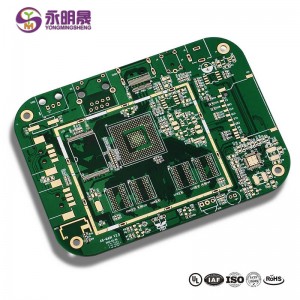
Learn more about YMS products
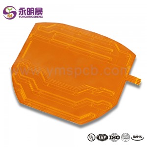
Flexible PCB 2Layer
Selective Hard Gold PCB
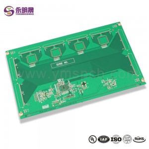
High Frequency PCBs manufacturing
PCB manufacturing
Read more news
3. How to make aluminum PCB boards
Video
heavy copper pcb 4 Layer (4/4/4/4OZ) Black Soldermask Board| YMS PCB Related Video: