Flex rigid Board semi flex PCB Black Soldermask| YMSPCB
Product Detail
What is Semi-Flex PCB?
The most traditional manufacturing process of semi-flex PCB is adopting the bending FR-4 materials and making PCB according to the traditional rigid PCB manufacturing process, and then using the deep milling technology to thin the areas that need to be bended so that it has a certain degree of flexibility, so as to meet the requirements of assembly bending connection.
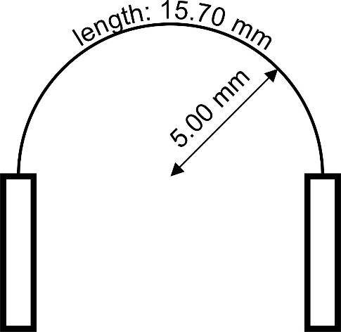
SEMI-FLEX length Calculator: (2 x Π x bend radius) x (bend angle/360°)
For example, bending 5 times over an angle of 180 degree with a radius of 5mm requires a minimum length of the semi-flex part of 15,7mm
YMS Semi-Flex PCB manufacturing capabilities:
| YMS Semi-Flex PCB manufacturing capabilities overview | ||
| Feature | capabilities | |
| Layer Count | 2-20L,with 1 – 2 conductive layers in the flexible section | |
| Rigid-Flex Thickness | 0.5mm-5.0mm | |
| PCB thickness in flex section | 0.15-0.8mm ± 0.05mm | |
| copper Thickness | 1/4OZ-10OZ | |
| Minimum line Width and Space | 0.05mm/0.05mm(2mil/2mil) | |
| Stiffeners | Stainless steel,PI, FR4 ,Aluminum etc. | |
| Material | FR4,RA copper, HTE copper, adhesive,Bondply,coverlayer, flex soldermask | |
| Min mechanical Drilled Size | 0.15mm(6mil) | |
| Min laser Holes Size: | 0.075mm(3mil) | |
| Surface Finish | Suitable Microwave/RF PCB urface finishes: Electroless Nickel, Immersion Gold, ENEPIG, Lead free HASL,Immersion Silver.etc. | |
| Solder Mask | Green, Red, Yellow, Blue, White, Black, Purple, Matte Black, Matte green.etc. | |
| Covrelay (Flex Part) | Yellow Coverlay, WhiteCoverlay,Black Coverlay |
|
Learn more about YMS products
Aluminum base pcb
Double Layer PCB
Mutilayer PCB Selective Hard Gold
Read more news
Product Tags
Flex rigid Board semi flex PCB Black Soldermask| YMSPCB Related Video:


