China Wholesale China LED Main Board House Appliance HDI Multilayer PCB
We’re committed to furnishing easy,time-saving and money-saving one-stop purchasing support of consumer for China Wholesale China LED Main Board House Appliance HDI Multilayer PCB, “Quality”, “honesty” and “service” is our principle. Our loyalty and commitments remain respectfully at your provider. Make contact with Us Today For more data, make contact with us now.
We’re committed to furnishing easy,time-saving and money-saving one-stop purchasing support of consumer for China PCB Board, Double Side PCB, Our Company policy is “quality first, to be better and stronger, sustainable development” . Our pursuit goals is “for society, customers, employees, partners and enterprises to seek reasonable benefit”. We aspirate to do cooperate with all different the auto parts manufacturers, repair shop, auto peer , then create a beautiful future! Thank you for taking time to browse our website and we would welcome any suggestions you may have that can help us to improve our site.
What is HDI PCB
HDI PCB: High density interconnect PCB, are a way of making more room on your printed circuit board to make them more efficient and allow for faster transmission. It’s relatively easy for most enterprising companies that are using printed circuit boards to see how this can benefit them.
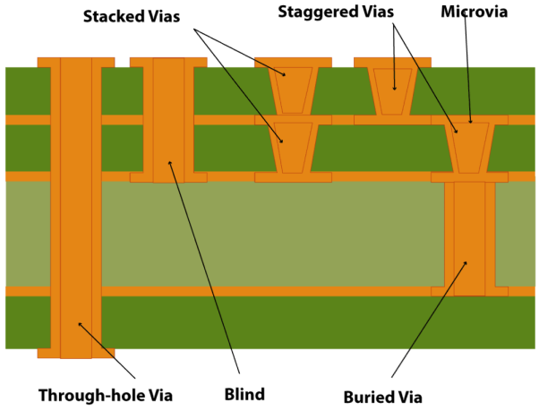
Advantages of HDI PCB
The most common reason for using HDI technology is a significant increase in packaging density. The space obtained by finer track structures is available for components. Besides, overall space requirements are reduced will result in smaller board sizes and fewer layers.
Usually FPGA or BGA are available with 1mm or less spacing. HDI technology makes routing and connection easy, especially when routing between pins.
YMS HDI PCB manufacturing capabilities:
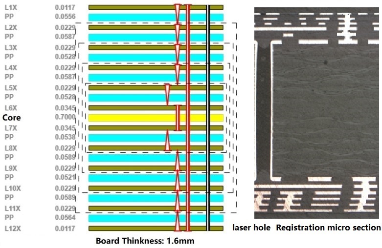
| YMS HDI PCB manufacturing capabilities overview | |
| Feature | capabilities |
| Layer Count | 4-60L |
| Available HDI PCB Technology | 1+N+1 |
| 2+N+2 | |
| 3+N+3 | |
| 4+N+4 | |
| 5+N+5 | |
| Any layer | |
| Thickness | 0.3mm-6mm |
| Minimum line Width and Space | 0.05mm/0.05mm(2mil/2mil) |
| BGA PITCH | 0.35mm |
| Min laser Drilled Size | 0.075mm(3nil) |
| Min mechanical Drilled Size | 0.15mm(6mil) |
| Aspect Ratio for laser hole | 0.9:1 |
| Aspect Ratio for through hole | 16:1 |
| Surface Finish | HASL, Lead free HASL,ENIG,Immersion Tin, OSP, Immersion Silver, Gold Finger, Electroplating Hard Gold, Selective OSP,ENEPIG.etc. |
| Via Fill Option | The via is plated and filled with either conductive or non-conductive epoxy then capped and plated over |
| Copper filled, silver filled | |
| Laser via copper plated shut | |
| Registration | ±4mil |
| Solder Mask | Green, Red, Yellow, Blue, White, Black, Purple, Matte Black, Matte green.etc. |
China Wholesale China LED Main Board House Appliance HDI Multilayer PCB Related Video: