High Quality for Ceramic Insulation Board - Multilayer PCB buried and blind via Halogen Free VIPPO IST test | YMSPCB – Yongmingsheng
What is Multilayer PCBs
Multilayer Printed Circuit Board, It is a type of PCB which comes with a combination of single sided PCB and double sided PCB. It features layers more than double sided PCB.
Benefits of Multilayer PCBs (compared to single or double-sided PCBs)
- Higher assembly density
- Smaller size (considerable savings on space)
- Increased flexibility
- Easier incorporation controlled impedance features.
- EMI shielding through careful placement of power and ground layers.
- Reduces the need for interconnection wiring harnesses (reduces overall weight)
Building a Multilayer PCB
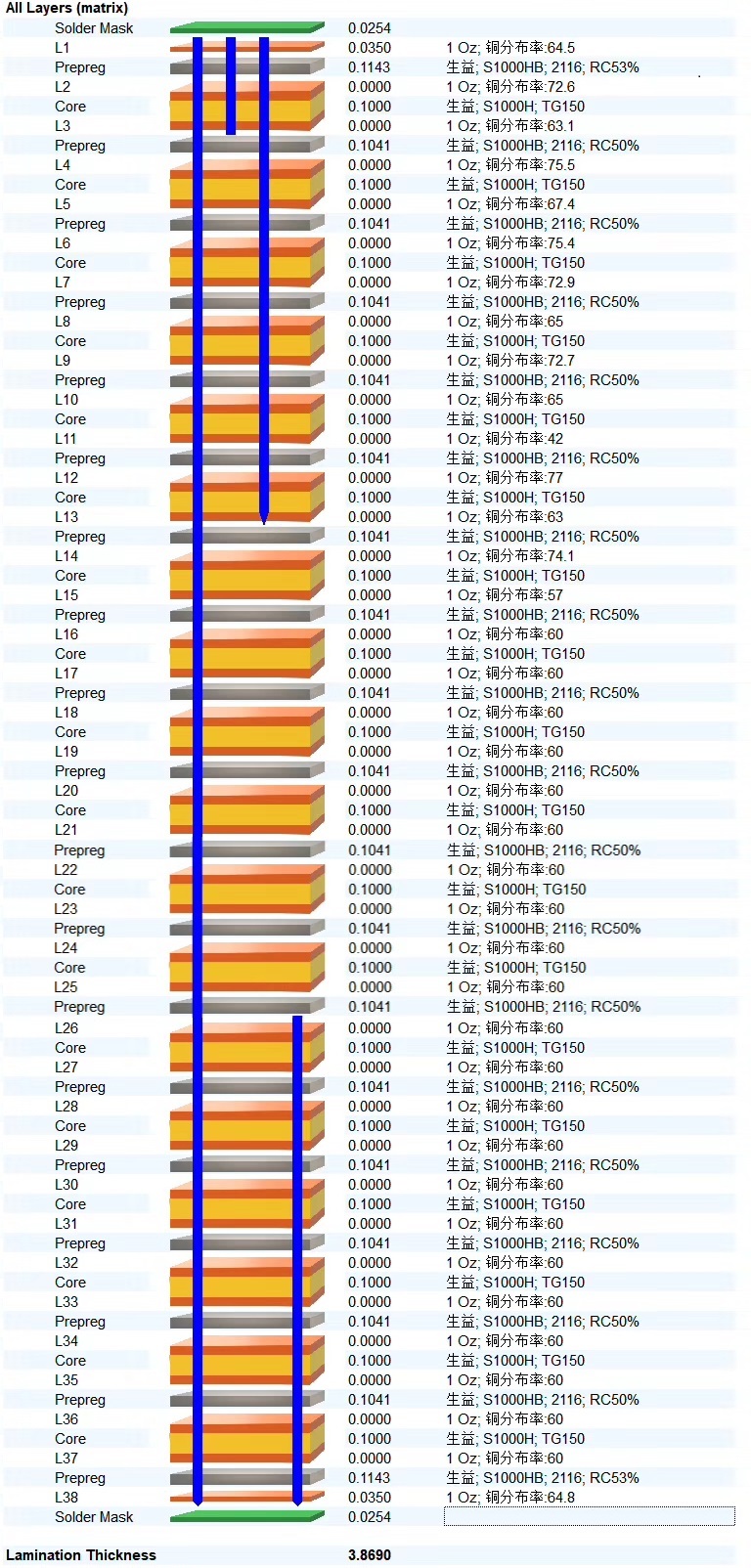
Multilayer PCBs are built by joining all the number of layers and materials at high temperature and pressure so as to remove any trapped air between the layers. Resin and adhesive material is used to stick the components and different layers together. You can choose from a number of materials such as exotic ceramic, epoxy glass, or Teflon etc. to build your PCB. The different prepreg and core layers are combined and go through the lamination process taking place at high temperature and pressure that helps to melt the layers together. After that the PCB is cooled down to form a hard and solid board.
YMS Multilayer PCB manufacturing capabilities:
| YMS Multilayer PCB manufacturing capabilities overview | ||
| Feature | capabilities | |
| Layer Count | 3-60L | |
| Available Multilayer PCB Technology | Through hole with Aspect Ratio 16:1 | |
| buried and blind via | ||
| Hybrid | High Frequency Material such as RO4350B and FR4 Mix etc. | |
| High Speed Material such as M7NE and FR4 Mix etc. | ||
| Thickness | 0.3mm-8mm | |
| Minimum line Width and Space | 0.05mm/0.05mm(2mil/2mil) | |
| BGA PITCH | 0.35mm | |
| Min mechanical Drilled Size | 0.15mm(6mil) | |
| Aspect Ratio for through hole | 16:1 | |
| Surface Finish | HASL, Lead free HASL,ENIG,Immersion Tin, OSP, Immersion Silver, Gold Finger, Electroplating Hard Gold, Selective OSP,ENEPIG.etc. | |
| Via Fill Option | The via is plated and filled with either conductive or non-conductive epoxy then capped and plated over(VIPPO) | |
| Copper filled, silver filled | ||
| Registration | ±4mil | |
| Solder Mask | Green, Red, Yellow, Blue, White, Black, Purple, Matte Black, Matte green.etc. | |
High Quality for Ceramic Insulation Board - Multilayer PCB buried and blind via Halogen Free VIPPO IST test | YMSPCB – Yongmingsheng Related Video: