Hot Selling for Hcpv Solar Thermal Ceramic Substrate - Discount Price China “Custom PCB Rogers Circuit Board Single /Double Sidecopper-Clad Laminate Aluminum PCB Board PCB Board Bvh High Frequency HDI Mpedance Control PCB Impedance B – Yongmingsheng
We now have quite a few superb workers customers very good at marketing and advertising, QC, and working with forms of troublesome dilemma while in the creation approach for Discount Price China “Custom PCB Rogers Circuit Board Single /Double Sidecopper-Clad Laminate Aluminum PCB Board PCB Board Bvh High Frequency HDI Mpedance Control PCB Impedance B, Welcome to arrange long-term marriage with us. Most effective Selling price Forever Quality in China.
We now have quite a few superb workers customers very good at marketing and advertising, QC, and working with forms of troublesome dilemma while in the creation approach for Best Selling Accept Customized, China Low Price Turnkey PCBA, Upon today, we have customers from all over the world, including USA, Russia, Spain, Italy, Singapore, Malaysia, Thailand, Poland, Iran and Iraq. The mission of our company is to provide the highest quality products with best price. We are looking forward to doing business with you!
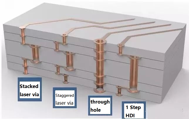
What is HDI PCBs?
High density interconnect (HDI) PCBs represent one of the fastest-growing segments of the printed circuit board market. Because of its higher circuitry density, the HDI PCB design can incorporate finer lines and spaces, smaller vias and capture pads, and higher connection pad densities. A high-density PCB features blind and buried vias and often contains microvias that are .006 in diameter or even less.
1.Multi-step HDI enables the connection between any layers;
2.Cross-layer laser processing can enhance the quality level of multi-step HDI;
3.The combination of HDI and high-frequency materials, metal-based laminates, FPC and other special laminates and processes enable the needs of high density and high frequency, high heat conducting, or 3D assembly.
YMS HDI PCB manufacturing capabilities:
| YMS HDI PCB manufacturing capabilities overview | |
| Feature | capabilities |
| Layer Count | 4-60L |
| Available HDI PCB Technology | 1+N+1 |
| 2+N+2 | |
| 3+N+3 | |
| 4+N+4 | |
| 5+N+5 | |
| Any layer | |
| Thickness | 0.3mm-6mm |
| Minimum line Width and Space | 0.05mm/0.05mm(2mil/2mil) |
| BGA PITCH | 0.35mm |
| Min laser Drilled Size | 0.075mm(3nil) |
| Min mechanical Drilled Size | 0.15mm(6mil) |
| Aspect Ratio for laser hole | 0.9:1 |
| Aspect Ratio for through hole | 16:1 |
| Surface Finish | HASL, Lead free HASL,ENIG,Immersion Tin, OSP, Immersion Silver, Gold Finger, Electroplating Hard Gold, Selective OSP,ENEPIG.etc. |
| Via Fill Option | The via is plated and filled with either conductive or non-conductive epoxy then capped and plated over |
| Copper filled, silver filled | |
| Laser via copper plated shut | |
| Registration | ±4mil |
| Solder Mask | Green, Red, Yellow, Blue, White, Black, Purple, Matte Black, Matte green.etc. |
Hot Selling for Hcpv Solar Thermal Ceramic Substrate - Discount Price China “Custom PCB Rogers Circuit Board Single /Double Sidecopper-Clad Laminate Aluminum PCB Board PCB Board Bvh High Frequency HDI Mpedance Control PCB Impedance B – Yongmingsheng Related Video:
