Hot Selling for Hcpv Solar Thermal Ceramic Substrate - multilayer pcb manufacturing High Tg material VIPPO| YMSPCB – Yongmingsheng
Product Detail
What is A Multilayer PCB?
Multilayer PCB boards came into play with the intention of constructing more number of conductive layers on the board than single layer or double layer boards. Multi-layer boards come with a combination of single layer or double layer board and give opportunity to connect more electronic components in less space.
YMS Multilayer PCB manufacturing capabilities:
| YMS Multilayer PCB manufacturing capabilities overview | ||
| Feature | capabilities | |
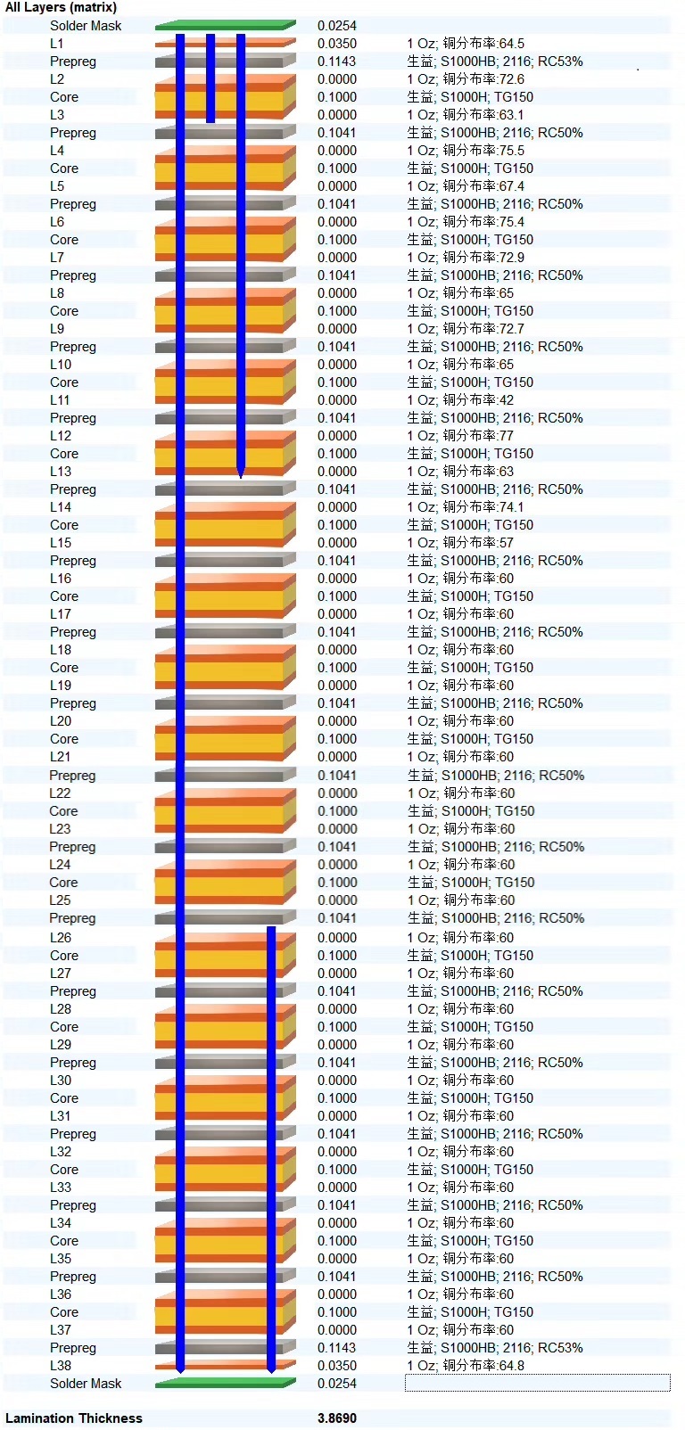
| Layer Count | 3-60L | |
| Available Multilayer PCB Technology | Through hole with Aspect Ratio 16:1 | |
| buried and blind via | ||
| Hybrid | High Frequency Material such as RO4350B and FR4 Mix etc. | |
| High Speed Material such as M7NE and FR4 Mix etc. | ||
| Thickness | 0.3mm-8mm | |
| Minimum line Width and Space | 0.05mm/0.05mm(2mil/2mil) | |
| BGA PITCH | 0.35mm | |
| Min mechanical Drilled Size | 0.15mm(6mil) | |
| Aspect Ratio for through hole | 16:1 | |
| Surface Finish | HASL, Lead free HASL,ENIG,Immersion Tin, OSP, Immersion Silver, Gold Finger, Electroplating Hard Gold, Selective OSP,ENEPIG.etc. | |
| Via Fill Option | The via is plated and filled with either conductive or non-conductive epoxy then capped and plated over(VIPPO) | |
| Copper filled, silver filled | ||
| Registration | ±4mil | |
| Solder Mask | Green, Red, Yellow, Blue, White, Black, Purple, Matte Black, Matte green.etc. | |
Product Tags
Hot Selling for Hcpv Solar Thermal Ceramic Substrate - multilayer pcb manufacturing High Tg material VIPPO| YMSPCB – Yongmingsheng Related Video: