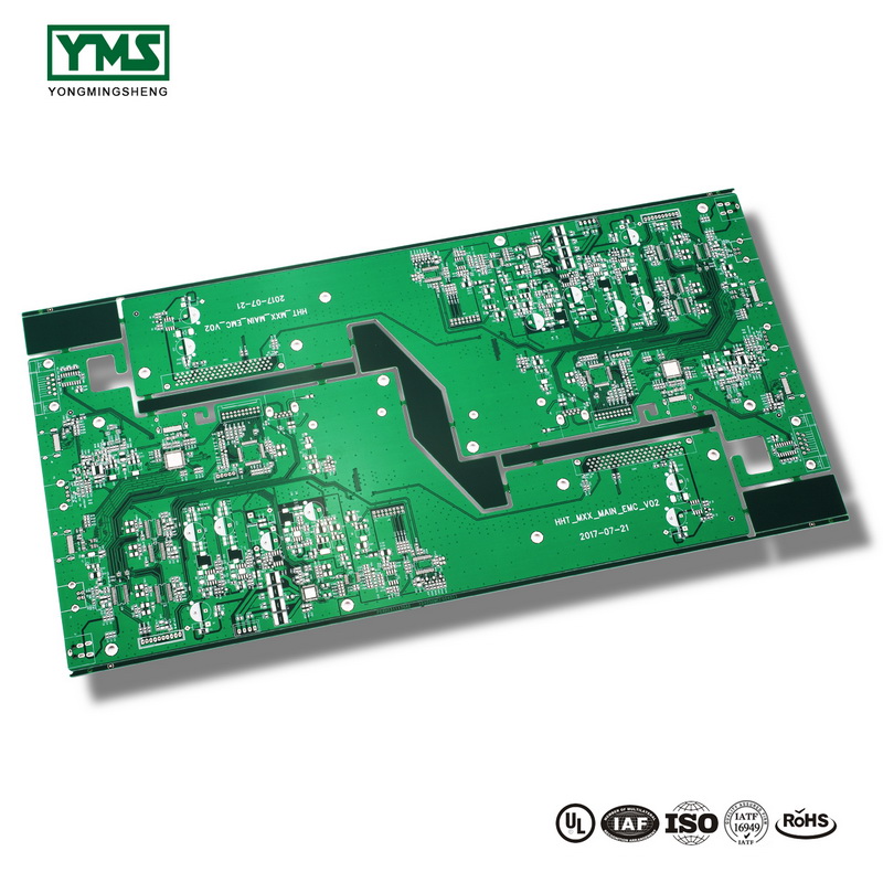
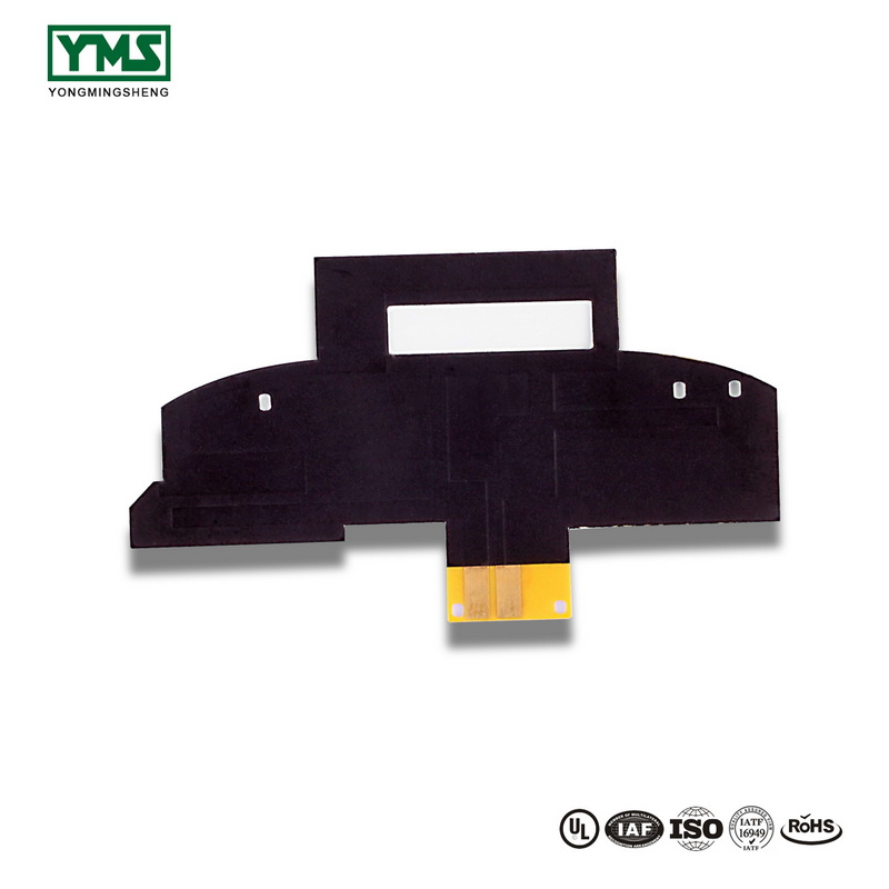
What is PCB proofing and PCB proofing detailed process
The so-called “PCB proofing” refers to the trial production of printed circuit board before mass production. The main application is the process that electronic engineers conduct small batch trial production to the factory after designing the circuit and completing the PCB.
This process belongs to the product design before the completion of confirmation and testing, which we understand as “PCB proofing”.
PCB proofing detailed process
1. Contact the manufacturer
Need to tell manufacturer of document, technological requirement, quantity above all.
Take China yongmingsheng PCB factory as an example, first enter yongmingsheng, then register the customer number, and then there will be professionals to quote, order and follow up the production schedule for you.
2. Laminate Shear
Objective: according to the requirements of engineering data MI, cut into small pieces on the large sheets meeting the requirements.Small pieces of sheet material that meet customer requirements.
Process: plate material → press MI requirement to cut plate → curium plate → beer round corner \ edge grinding → plate
3. Drill
Objective: according to the engineering data, drill the hole diameter in the corresponding position on the sheet metal with the required size.
Process: lamination pin → upper plate → drilling → lower plate → inspection \ repair
4. PTH
Objective: to deposit a thin layer of copper on the wall of insulating hole by chemical method.
Process: rough grinding → hanging plate → sink copper automatic line → lower plate → dip 1% dilute H2SO4→ thicken copper
5. Outer Layer
Purpose: graphic transfer is the transfer of images from the production film to the board
Process: (blue oil process) : grinding plate → first side of printing → drying → second side of printing → drying → blasting light → impact → inspection;(dry film process) : hemp plate → pressing film → static setting → alignment → exposure → static setting → impact → inspection
6. Pattern Plating
Objective: graphic electroplating is to electroplate a copper layer of required thickness and a gold nickel or tin layer of required thickness on the exposed copper skin or hole wall.
Process: upper plate → deoiling → washing twice → microerosion → washing → pickling → copper plating → washing → pickling → acid dipping → tin plating → washing → lower plate
7. Adhesive Remove
Objective: to use NaOH solution to remove anti – electroplating coating layer to expose non – line copper layer.
Process: water film: frame → leaching → washing → scrubbing → passing machine;Dry film: put plate → pass machine
8. Etching
Objective: etching is to use chemical reaction method to corrode the copper layer in non-circuit parts.
9. Solder Mask
Objective: green oil is to transfer the green oil film to the board, which can protect the circuit and prevent the tin on the circuit when welding parts
Process: grinding plate → printing photosensitive green oil → curium plate → exposure → impact;Mill plate → press the first side → dry plate → press the second side → dry plate
10. Silk Sreen
Purpose: a character is a token provided for easy identification
Process: green oil terminal curium → cooling static → network adjustment → printed characters → curium
11. Gold-plated fingers
Objective: to coat the finger of the plug with a layer of required thickness of nickel \ gold to make it more durable
Process: upper plate → deoiling → washing twice → micro-corrosion → washing twice → pickling → copper plating → washing → nickel plating → washing → gold plating
Tinplate (a process of juxtaposition)
Objective: tin spraying is to spray a layer of lead tin on the exposed copper surface which is not covered with welding resistance oil, so as to protect the copper surface from corrosion and oxidation and ensure good welding performance.
Process: micro erosion → air drying → preheating → rosin coating → solder coating → hot air leveling → air cooling → washing air drying
12.Final Shaping
Objective: through the die stamping or CNC gong machine gong shape molding method of organic gong, beer plate, hand gong, hand cut
The accuracy of the data gong machine board and beer board is higher, the second hand gong, the lowest hand cutting board can only do some simple shape.
13. Electrical Test
Objective: through the electronic 100% test, to detect the open circuit, short circuit and other defects that affect the function.
Process: upper die → place plate → test → pass →FQC inspection → unqualified → repair → return test →OK→REJ→ scrap
14. Final Quality Control
Objective: through 100% visual inspection of the plate appearance defects, and to repair minor defects, avoid problems and defects of the plate outflow.
Specific workflow: incoming materials → view data → visual inspection → qualified →FQA spot check → qualified → packaging → unqualified → processing → inspection OK
Yongmingsheng is a professional PCB manufacturing factory. We are from China. You are welcome to contact us

