What is the meaning of PCB board and PCB board skills
What is the definition of PCB board
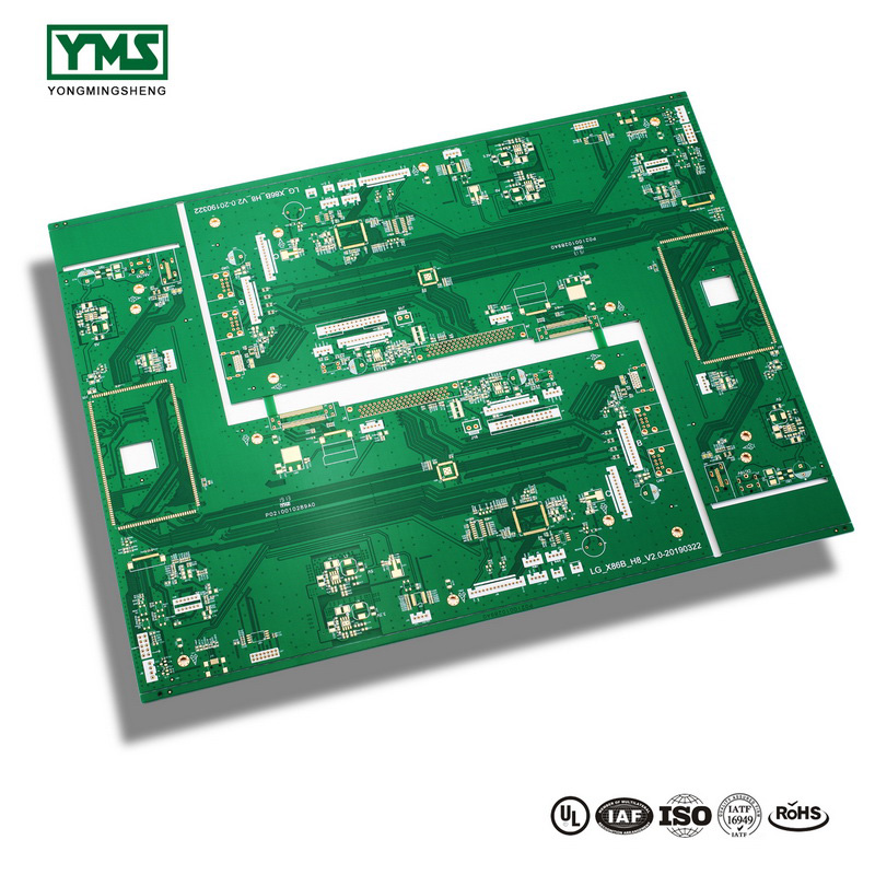
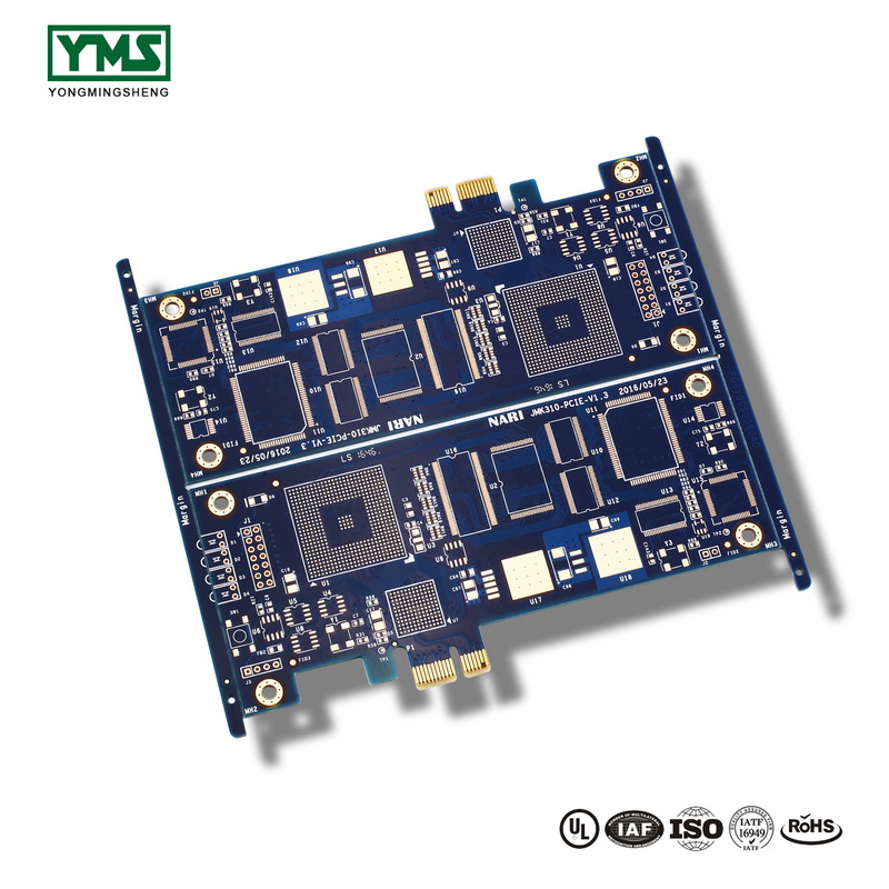
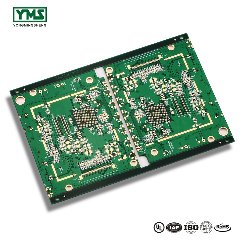
PCB board is just for the convenience of production. For the plate factory, its substrate is usually relatively large, making many boards at one time, and then cutting them off one by one. If panel is primarily used for welding production, imagine a nail-sized board welded one by one onto an SMT machine as big as a car.
PCB board has several definitions!
Convenient customer plug-in , convenient manufacturer their production and saving material!
The convenience plug-in is what the customer requires, and you have to do it. The factory is convenient for production is convenient for V-CUT.
Saving materials is to more perfect use of materials and not waste or leave too much edge material! For example, for a material of 1.2 meters by 1 meter, you can open a 34X41 CM panel and it will be perfect.
PCB panel method
The PCB panel method includes the method of using Excel program stored in the public computer to create the finished jigsaw worksheet and the raw jigsaw worksheet, as well as the use method of the said worksheet. The work sheet of finished board is used to complete the process of the finished board on the blank board. Each column, the finished plate makeup worksheet cell used for placing different billet board makeup scheme of the same categories of data or the data of Excel formula of internal function, every line of cell is used to place the same makeup scheme of different categories of data or the data of Excel formula of internal function, to create the finished plate makeup work table of the specific method is:
(1) Start the Excel program stored in the public computer, create a new workbook, and select a worksheet.
(2) Enter the name of the worksheet with a cell in the table.
(3) Use a row of cells in the table as the header of the worksheet, and enter the category name of the data in its column in each cell.
(4) Create data input area.
(5) Create data operation area.
(6) Create data output area.
(7) Create a jigsaw operation area.
(8) Create the indirect output area and use Excel internal lookup and reference functions to refer to all the data in the worksheet of the jigsaw operation area and place it in the indirect output area.
PCB panel skill
PCB panel is the thing that PCB factory often wants to do, what matters need to pay attention to when carrying out panel? What are the requirements of PCB panel? To sum up for you:
First is the problem of panel. We know that the main problem of panel is to save production cost. For PCB board width ≤260mm ~ 300mm, depending on the production line. Because we may have a lot of materials, the processing equipment of one material gun corresponds to one module, so if the panel exceeds the range of modules, the processing speed will be very slow.
The outer frame (clamping edge) of the PCB assembly board should be carefully considered to ensure that the PCB assembly board will not be deformed after it is fixed on the fixture (v-slot on this edge is generally not allowed). For the layout of components, first, all orientations should be consistent, without mirroring, which will cause the problem of coordinate positioning of machining.
Second, there should be no connector protruding from the edge (between the outer frame and the inner panel, and between the panels and the panels). If there is such a situation, it will hinder the cutter plate splitting after the completion of welding.
In order to ensure the position and level of the detection panel, we need to set more than three registration points on the edge of the panel. Through optical detection of these three points, the reference coordinate of the whole processing and the levelness of the panel can be obtained.
The correct approach is: the distance is different when the edge is 5mm away from the edge and the direction of travel is not consistent (easy to distinguish the direction of entry) : [when setting the reference anchor point, a 1.5mm larger than the anchor point is usually reserved around the anchor point, and similar pads or other similar pads are not allowed]
There should be at least three positioning holes in each small plate, 3≤ aperture ≤6 mm, no wiring or patch is allowed within 1mm of edge positioning hole (to prevent misjudgment). PCB panel is mainly to save production and processing costs (will make the machine processing speed several times faster), unreasonable design will make the later stage full of problems, you can take a careful look to prevent problems.
First is the problem of panel. We know that the main problem of jigsaw board is to save production cost. For PCB panel width ≤260mm ~ 300mm, depending on the production line. Because we may have a lot of materials, the processing equipment of one material gun corresponds to one module, so if the panel exceeds the range of modules, the processing speed will be very slow.
Yongmingsheng is a professional PCB manufacturing factory. We are from China. You are welcome to contact us


