Double sided PCB standard pcb Countersink manufacturers | YMSPCB
Printed Circuit Board Introduction
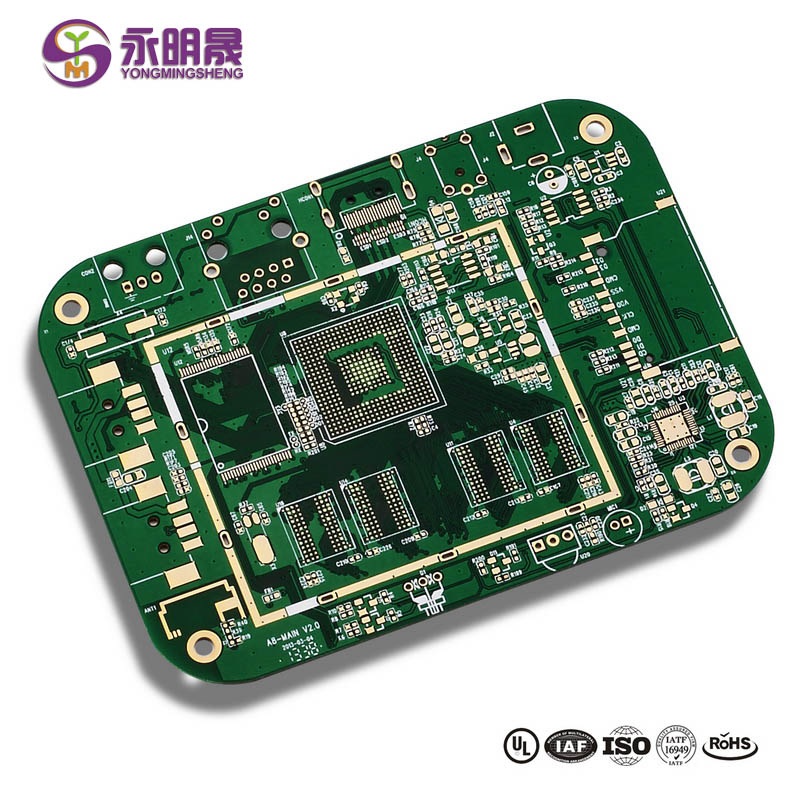
A printed circuit board (PCB) mechanically supports and electrically connects electrical or electronic components using conductive tracks, pads and other features etched from one or more sheet layers of copper laminated onto and/or between sheet layers of a non-conductive substrate. Components are generally soldered onto the PCB to both electrically connect and mechanically fasten them to it.PCBs can be single-sided (one copper layer), double-sided (two copper layers on both sides of one substrate layer), or multi-layer (outer and inner layers of copper, alternating with layers of substrate). Multi-layer PCBs allow for much higher component density, because circuit traces on the inner layers would otherwise take up surface space between components. The rise in popularity of multilayer PCBs with more than two, and especially with more than four, copper planes was concurrent with the adoption of surface mount technology.
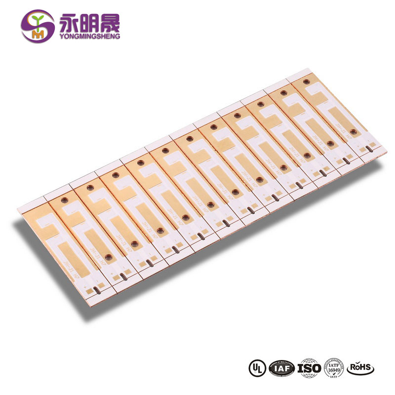
Double-sided circuit boards are a little bit more complex than single sided PCB. These boards contain just a single layer of the base substrate. However, they contain conductive layers on each side. They use copper as a conductive material. Let’s dive deeper inside double sided PCB to learn more!
The Structure and Materials of Double Sided PCB
Double sided PCB material can vary on the basis of project type. However, the core material is almost the same for all circuit boards. However, the structure of the PCB varies from type to type.
Substrate: It is the most important material made of fiberglass. You can consider it as a skeleton of the PCB.
Copper Layer: It can be either foil or full copper coating. That’s why it depends on board type. The end result is the same whether you use foil or copper coating. Double sided circuit boards contain a conductive copper layer on both sides.
Solder Mask: It is a protective layer of polymer. So, it prevents copper from short-circuiting. You can consider it as the skin of the circuit board. Double sided PCB soldering is a very important step for durability.
Silkscreen: it is the final part of silkscreen. Although it doesn’t have any role in the functionality of the circuit board. Manufacturers use it to show part numbers. Part numbers are very important for testing purposes. In addition, you can print your company logos or other information in the form of text.
The Advantages and Disadvantages of Double Sided Circuit Boards
Here are some pro and cons of double-sided printed circuit boards:
Advantages of Double-sided Circuit Boards
High Quality: Planning and designing this PCB need a good amount of work. Resulting in high-quality circuit boards.
Enough Space for Components: It houses more space for components. Because both sides of the layer are conductive.
More Design Options: It has conductive layers on both sides. You can attach different electronic components on both sides. So you have more design options.
Sourcing and Sinking Current: While using it as a bottom layer, you can use it for sinking and sourcing current.
Usage: Due to its efficiency, you can use it in many applications.
Disadvantages of Double-sided Circuit boards
Higher Cost: Making both sides conductive, it comes at a slightly higher cost.
Skilled Designer Needed: There involves a bit difficult double sided PCB manufacturing process for its formation. Therefore, you need more proficient engineers for its productions.
Production Time: Production time is more than a single sided PCB due to its complexity.
Application of Double Sided Circuit Boards
This type of circuit board increases circuit density. They are more flexible as well. Almost all double sided PCB manufacturers use it in many electronic gadgets. Below is some remarkable use case of double-sided circuit boards:
HVAC and LED lighting
Traffic control system
Automotive dashboards
Control relays and Power conversion
Regulators and power supplies
To test and monitor different equipment
Printers and cellphone systems
Vending machines.

YMS Normal PCB manufacturing capabilities:
| YMS Normal PCB manufacturing capabilities overview | ||
| Feature | capabilities | |
| Layer Count | 1-60L | |
| Available Normal PCB Technology | Through hole with Aspect Ratio 16:1 | |
| buried and blind via | ||
| Hybrid | High Frequency Material such as RO4350B and FR4 Mix etc. | |
| High Speed Material such as M7NE and FR4 Mix etc. | ||
| Material | CEM- | CEM-1;CEM-2;CEM-4;CEM-5.etc |
| FR4 | EM827, 370HR, S1000-2, IT180A, IT158, S1000 / S1155, R1566W, EM285, TU862HF,NP170G etc. | |
| High Speed | Megtron6, Megtron4, Megtron7,TU872SLK, FR408HR,N4000-13 Series,MW4000,MW2000,TU933 etc. | |
| High Frequency | Ro3003, Ro3006, Ro4350B, Ro4360G2, Ro4835, CLTE, Genclad, RF35, FastRise27 etc. | |
| Others | Polyimide, Tk, LCP, BT, C-ply, Fradflex, Omega , ZBC2000,PEEK,PTFE,ceramic-based etc. | |
| Thickness | 0.3mm-8mm | |
| Max.copper Thickness | 10OZ | |
| Minimum line Width and Space | 0.05mm/0.05mm(2mil/2mil) | |
| BGA PITCH | 0.35mm | |
| Min mechanical Drilled Size | 0.15mm(6mil) | |
| Aspect Ratio for through hole | 16:1 | |
| Surface Finish | HASL, Lead free HASL,ENIG,Immersion Tin, OSP, Immersion Silver, Gold Finger, Electroplating Hard Gold, Selective OSP,ENEPIG.etc. | |
| Via Fill Option | The via is plated and filled with either conductive or non-conductive epoxy then capped and plated over(VIPPO) | |
| Copper filled, silver filled | ||
| Registration | ±4mil | |
| Solder Mask | Green, Red, Yellow, Blue, White, Black, Purple, Matte Black, Matte green.etc. | |
Video
Learn more about YMS products
Selective Hard Gold PCB
Bendable Printed Circuit Board
Flex rigid pcb
Multilayer pcb
Metal clad pcb
Read more news
Double sided PCB standard pcb Countersink manufacturers | YMSPCB Related Video: