Professional Design Electriplating Filling Pcb - High TG PCB 6Layer Gold Finger Blue Soldermask Board| YMS PCB – Yongmingsheng
What is High-Tg circuit boards (HTg)?
High Tg refers to high heat resistance.Generally, the boards of Tg are over 130 degrees, high Tg is generally greater than 170 degrees, and medium Tg is about greater than 150 degrees. Generally, PCB printed boards with Tg≥170℃ are called high Tg printed boards.
High Tg materials have the following properties:
- High glass flow temperature value (Tg)
- High temperature durability
- Long delamination durability
- Low Z axis expansion (CTE)
Goldfinger design in PCB
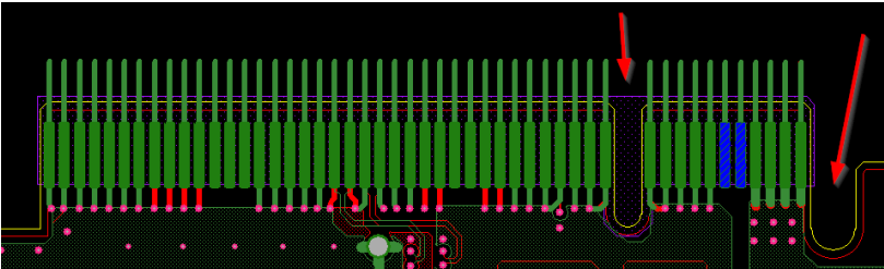
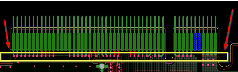
Goldfinger is an electrical interface. The common packaging form and appearance of PCB are as follows. When the appearance and packaging similar to the figure below are seen in the PCB design, the first reaction is to see them on the boardGold finger.
The easier way for goldfinger to judge is to have both the TOP and BOTTOM of the device
PIN device;It will look like the u-slot in the picture below.
When there is a goldfinger on the board, you need to work on the details of the goldfinger.
Details of goldfinger in PCB:
1) in order to increase the wear resistance of goldfinger, goldfinger usually needs to be plated with hard gold.
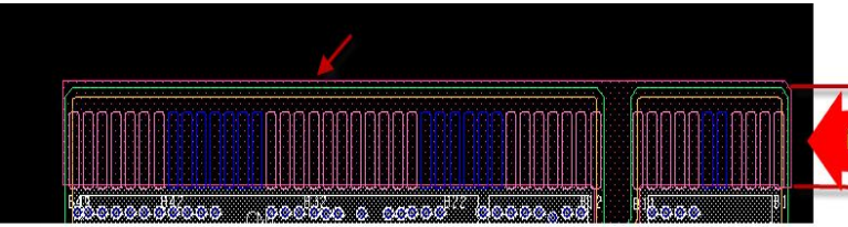
2) goldfinger needs chamfering, usually 45°, other angles such as 20°, 30°, etc.
If there is no chamfer in the design, there is a problem.In the figure below, the arrow is 45 degrees
chamfering
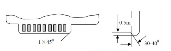
The 45° chamfering Angle in PCB is shown in the following figure:
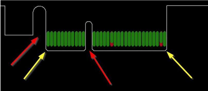
3) goldfinger needs to do the whole block of anti-welding window opening treatment, and the PIN does not need to open the steel net;
4) a minimum distance of 14mil from the tip of finger is required for the sink tin and silver welding pads;Recommended design
When the pad is more than 1mm away from the finger position, including the through hole pad;
5) do not coat goldfinger with copper;
Below is a goldfinger design for reference
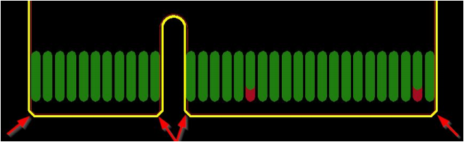
6) all layers of the inner layer of goldfinger need to be copper whittled, usually with a width of 3mm;
It can be done with half finger and whole finger.In pci-e design, there are also fingers
Remove all copper from the mingoldfinger area;
Goldfinger’s resistance will be low, and cupping (hollowing out under the finger) will reduce it
The impedance difference between the impedance line and the impedance line is also beneficial to ESD.
Suggestion: cut all the copper under the goldfinger welding pad
YMS High Tg PCB manufacturing capabilities:
|
YMS High Tg PCB manufacturing capabilities overview |
||
| Feature | capabilities | |
| Layer Count | 3-60L | |
| Available Multilayer PCB Technology | Through hole with Aspect Ratio 16:1 | |
| buried and blind via | ||
| Hybrid | High Frequency Material such as RO4350B and FR4 TG 180°Mix etc. | |
| High Speed Material such as M7NE and FR4 TG 180°Mix etc. | ||
| Thickness | 0.3mm-8mm | |
| Minimum line Width and Space | 0.05mm/0.05mm(2mil/2mil) | |
| BGA PITCH | 0.35mm | |
| Min mechanical Drilled Size | 0.15mm(6mil) | |
| Aspect Ratio for through hole | 16:1 | |
| Surface Finish | HASL, Lead free HASL,ENIG,Immersion Tin, OSP, Immersion Silver, Gold Finger, Electroplating Hard Gold, Selective OSP,ENEPIG.etc. | |
| Via Fill Option | The via is plated and filled with either conductive or non-conductive epoxy then capped and plated over(VIPPO) | |
| Copper filled, silver filled | ||
| Registration | ±4mil | |
| Solder Mask | Green, Red, Yellow, Blue, White, Black, Purple, Matte Black, Matte green.etc. | |
Professional Design Electriplating Filling Pcb - High TG PCB 6Layer Gold Finger Blue Soldermask Board| YMS PCB – Yongmingsheng Related Video: