Multilayer PCB manufacturing from 4 to 60 Layers | YMSPCB
Product Detail
The multilayer PCB refers to a printed circuit board with more than two layers, which is composed of interconnected lines on several layers of insulating substrates and pads for assembling and soldering electronic components. It has the function of conducting each layer of lines and insulating each other. High-speed PCBs are generally designed with multilayer PCB. Common multilayer boards are generally 4-layer boards or 6-layer boards, and complex multi-layer boardscan reach dozens of layers.
YMS Multilayer PCB manufacturing capabilities:
| YMS Multilayer PCB manufacturing capabilities overview | ||
| Feature | capabilities | |
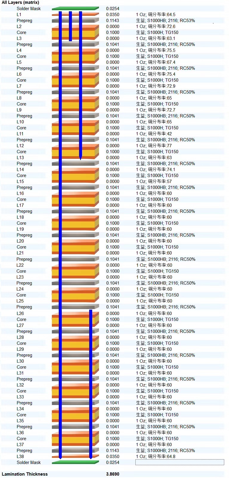
| Layer Count | 3-60L | |
| Available Multilayer PCB Technology | Through hole with Aspect Ratio 16:1 | |
| buried and blind via | ||
| Hybrid | High Frequency Material such as RO4350B and FR4 Mix etc. | |
| High Speed Material such as M7NE and FR4 Mix etc. | ||
| Thickness | 0.3mm-8mm | |
| Minimum line Width and Space | 0.05mm/0.05mm(2mil/2mil) | |
| BGA PITCH | 0.35mm | |
| Min mechanical Drilled Size | 0.15mm(6mil) | |
| Aspect Ratio for through hole | 16:1 | |
| Surface Finish | HASL, Lead free HASL,ENIG,Immersion Tin, OSP, Immersion Silver, Gold Finger, Electroplating Hard Gold, Selective OSP,ENEPIG.etc. | |
| Via Fill Option | The via is plated and filled with either conductive or non-conductive epoxy then capped and plated over(VIPPO) | |
| Copper filled, silver filled | ||
| Registration | ±4mil | |
| Solder Mask | Green, Red, Yellow, Blue, White, Black, Purple, Matte Black, Matte green.etc. | |
Learn more about YMS products

Stiffener Flex PCB Manufacturer

Rigid flex pcb single

multilayer pcb manufacturing

HDI pcb
Read more news
Product Tags
Multilayer PCB manufacturing from 4 to 60 Layers | YMSPCB Related Video: