Special Design for Thermoelectric Copper Base Pcb - High Quality for China Multilayer Fr-4 Blind Buried Hole Immersion Gold HDI PCB Printed Circuit Board – Yongmingsheng
That has a sound small business credit, great after-sales service and modern production facilities, we’ve earned an outstanding standing amid our buyers across the earth for High Quality for China Multilayer Fr-4 Blind Buried Hole Immersion Gold HDI PCB Printed Circuit Board, Aggressive price with good quality and satisfying services make us earned a lot more prospects.we wish to operate with you and request common improvement.
That has a sound small business credit, great after-sales service and modern production facilities, we’ve earned an outstanding standing amid our buyers across the earth for 94v0 Rohs Pcb Board, China PCB Circuit Boards, Our items are exported worldwide. Our customers are always satisfied with our reliable quality, customer-oriented services and competitive prices. Our mission is “to continue to earn your loyalty by dedicating our efforts to the constant improvement of our items and services in order to ensure the satisfaction of our end-users, customers, employees, suppliers and the worldwide communities in which we cooperate”.
HDI Board production process:
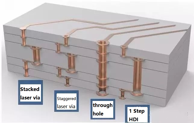
At present, HDI board interconnection between layer and layer is mainly the following design: Staggered holes interconnection, Cross-layer interconnection, ladder interconnection and superposition holes interconnection. Among them, the superposition holes interconnection occupy the least space. There is a research suggests that reducing the number of through holes and increasing the number of blind holes can effectively improve the wiring density. And in the superposition interconnection, the methods of electroplating and resin plug are mainly used, especially the electroplating hole filling method which has more obvious advantages like high reliability and good conduction performance. Therefore, superposition interconnection is the most widely used design method for blind holes design. The process of stacking between layers is as follows: first blind hole is made, then second blind hole is made after lamination, then multi-blind hole is made according to this method, and the interconnection between layers is realized by electroplating hole filling method.
On the whole, the production process of HDI plate is complex, which needs to be completed after many times of production for a long time. It’s not only high requirements for the accuracy and shrinkage control of each layer, but also high standards in materials, equipment, environment and technical personnel.
YMS HDI PCB manufacturing capabilities:
| YMS HDI PCB manufacturing capabilities overview | |
| Feature | capabilities |
| Layer Count | 4-60L |
| Available HDI PCB Technology | 1+N+1 |
| 2+N+2 | |
| 3+N+3 | |
| 4+N+4 | |
| 5+N+5 | |
| Any layer | |
| Thickness | 0.3mm-6mm |
| Minimum line Width and Space | 0.05mm/0.05mm(2mil/2mil) |
| BGA PITCH | 0.35mm |
| Min laser Drilled Size | 0.075mm(3nil) |
| Min mechanical Drilled Size | 0.15mm(6mil) |
| Aspect Ratio for laser hole | 0.9:1 |
| Aspect Ratio for through hole | 16:1 |
| Surface Finish | HASL, Lead free HASL,ENIG,Immersion Tin, OSP, Immersion Silver, Gold Finger, Electroplating Hard Gold, Selective OSP,ENEPIG.etc. |
| Via Fill Option | The via is plated and filled with either conductive or non-conductive epoxy then capped and plated over |
| Copper filled, silver filled | |
| Laser via copper plated shut | |
| Registration | ±4mil |
| Solder Mask | Green, Red, Yellow, Blue, White, Black, Purple, Matte Black, Matte green.etc. |
Special Design for Thermoelectric Copper Base Pcb - High Quality for China Multilayer Fr-4 Blind Buried Hole Immersion Gold HDI PCB Printed Circuit Board – Yongmingsheng Related Video:
