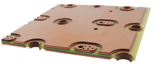
Super Purchasing for 3mil Printed Circuit Boards - heavy copper pcb 4 Layer (4/4/4/4OZ) Black Soldermask Board| YMS PCB – Yongmingsheng
Product Detail
What is heavy copper PCB?
This PCB classic is the first choice when high currents are unavoidable: the thick copper PCB, manufactured in genuine etching technology. Thick copper PCBs are characterised by structures with copper thicknesses from 105 to 400 µm. These PCBs are used for large (high) current outputs and for optimisation of the thermal management. The thick copper allows large PCB-cross-sections for high current loads and encourages heat dissipation. The most common designs are multilayer or double-sided.
YMS Heavy copper PCB manufacturing capabilities:
| YMS Heavy copper PCB manufacturing capabilities overview | ||
| Feature | capabilities | |
| Layer Count | 1-30L | |
| Base Material | FR-4 Standard Tg, FR4-mid Tg,FR4-High Tg | |
| Thickness | 0.6 mm – 8.0mm | |
| Maximum Outer Layer Copper Weight (Finished) | 15OZ | |
| Maximum Inner Layer Copper Weight (Finished) | 30OZ | |
| Minimum line Width and Space | 4oz Cu 8mil/8mil; 5oz Cu 10mil/10mil; 6oz Cu 12mil/12mil; 12oz Cu 18mil/28mil; 15oz Cu 30mil/38mil .etc. | |
| BGA PITCH | 0.8mm(32mil) | |
| Min mechanical Drilled Size | 0.25mm(10mil) | |
| Aspect Ratio for through hole | 16:1 | |
| Surface Finish | HASL, Lead free HASL,ENIG,Immersion Tin, OSP, Immersion Silver, Gold Finger, Electroplating Hard Gold, Selective OSP,ENEPIG.etc. | |
| Via Fill Option | The via is plated and filled with either conductive or non-conductive epoxy then capped and plated over(VIPPO) | |
| Copper filled, silver filled | ||
| Registration | ±4mil | |
| Solder Mask | Green, Red, Yellow, Blue, White, Black, Purple, Matte Black, Matte green.etc. | |
Product Tags
Super Purchasing for 3mil Printed Circuit Boards - heavy copper pcb 4 Layer (4/4/4/4OZ) Black Soldermask Board| YMS PCB – Yongmingsheng Related Video:
